Method for achieving accurate graphic positioning during observation using scanning electron microscope

An electron microscope and graphic positioning technology, applied in the field of semiconductor technology, can solve problems such as difficult positioning

Active Publication Date: 2014-02-05
SHANGHAI HUALI MICROELECTRONICS CORP
View PDF4 Cites 0 Cited by
  • Summary
  • Abstract
  • Description
  • Claims
  • Application Information

AI Technical Summary

Problems solved by technology

[0003] The invention discloses a method for precise pattern positioning in scanning electron microscope observation, which is used to solve the problem of difficult positioning in the prior art when observing structures with a large aspect ratio

Method used


Image

  • Method for achieving accurate graphic positioning during observation using scanning electron microscope
  • Method for achieving accurate graphic positioning during observation using scanning electron microscope

Examples


Embodiment Construction

[0016] The specific embodiment of the present invention will be further described below in conjunction with accompanying drawing:

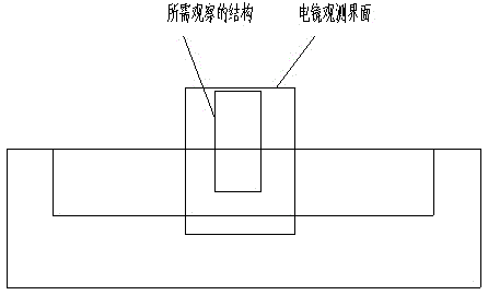
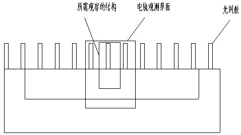
[0017] figure 2 It is a structural schematic diagram of the method for precise pattern positioning in scanning electron microscope observation of the present invention, please refer to figure 2 , a method for precise pattern positioning in scanning electron microscope observation, wherein a plurality of photoresist lines with the same width and parallel to each other are formed on the surface of a wafer, and the distance between any two adjacent photoresist lines is the same, A plurality of photoresist lines are used as a reference to accurately locate the structure to be observed on the wafer, and the position of the observation point in the structure to be observed can be accurately known through the above process.

[0018] The method for forming multiple photoresist lines in the present invention specifically includes: spin-coating the photo...


PUM


Abstract

The invention discloses a method for achieving accurate graphic positioning during observation using a scanning electron microscope, and solves the problem in the prior art that the positioning operation is difficult when a structure with a large depth-width ratio is observed. Photoresists are coated on the surface of a wafer, and then photoresist lines with fixed width and spacing are etched by using a specific mask. The photoresist lines serve as positioning markers for accurate positioning during observation using the scanning electron microscope. For the structure with a large depth-width ratio, the positions of observation points in the observed structure are accurately determined only by calculating the number of the photoresist lines on the surface of the wafer.

Description

technical field [0001] The invention relates to a semiconductor process, in particular to a method for precise pattern positioning in scanning electron microscope observation. Background technique [0002] The current scanning electron microscope section observation usually first observes the surface of the wafer sample with a small magnification, finds the pattern to be observed, and then uses a high magnification to observe the pattern structure. During this period, there is no fixed relative coordinate to define the position of the observation point. figure 1 It is a schematic diagram of scanning electron microscope observation in the prior art, please refer to figure 1 , this method has no problem in observing structures with a relatively close aspect ratio, but when observing structures with a large aspect ratio (the aspect ratio is often greater than 100), such as graphics for optical measurement, if you want to observe graphics A specific location, you will enco...

Claims


Application Information

Patent Timeline
Patent Type & Authority Patents(China)
IPC IPC(8): H01L21/311H01L23/544G03F7/00
Inventor 邓镭
Owner SHANGHAI HUALI MICROELECTRONICS CORP
Why Eureka
Try Eureka