Nonvolatile memory element and method for manufacturing same

A technology of non-volatile storage and manufacturing method, which is applied in the field of non-volatile storage elements and can solve the problems of uneven resistance value and the like

Inactive Publication Date: 2012-05-09
PANASONIC CORP
View PDF8 Cites 2 Cited by
  • Summary
  • Abstract
  • Description
  • Claims
  • Application Information

AI Technical Summary

Problems solved by technology

[0007] However, in the above-mentioned conventional variable resistance nonvolatile memory element, there is a problem that the actual resistance value non-uniformity (340% non-uniformity) exceeds that based on the film thickness and film composition of the variable resistance layer, electrodes, etc., and Unevenness in resistance value expected from the size and shape of the resist after lithography, or the shape after dry etching (14%)

Method used


Image

  • Nonvolatile memory element and method for manufacturing same
  • Nonvolatile memory element and method for manufacturing same
  • Nonvolatile memory element and method for manufacturing same

Examples


Embodiment approach 1

[0095] (Structure of non-volatile memory element)

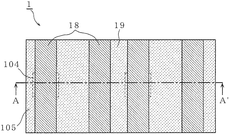
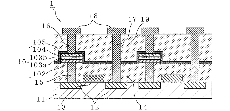
[0096] Figure 1A as well as Figure 1B It is a diagram showing the structure of the nonvolatile memory element according to Embodiment 1 of the present invention. Figure 1A represents a top view, Figure 1B Indicates looking in the direction of the arrow Figure 1A A cross-sectional view of the section of the line A-A'. Figure 1A as well as Figure 1B An example of a case where two variable resistance elements 10 are configured is shown. In this embodiment, an insulating layer that reduces stress is designed as the stress relaxation region layer 105 so as to cover at least the upper electrode layer 104 . Furthermore, the stress relaxation region layer 105 has a function of relieving stress at the interface between the upper electrode layer 104 and the second interlayer insulating layer 19 .

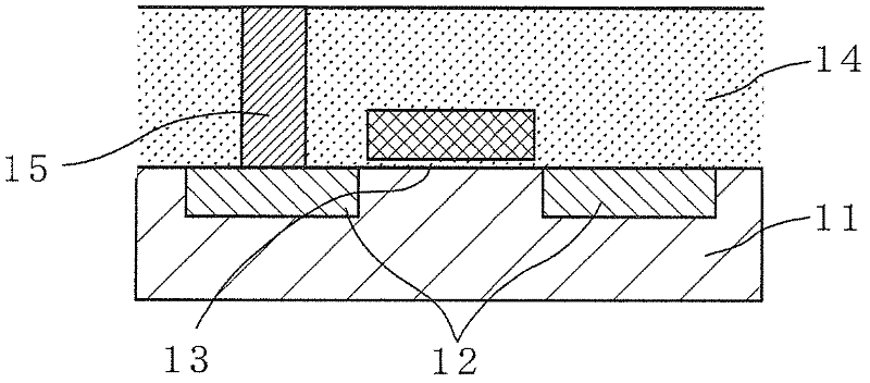
[0097] Figure 1B The shown nonvolatile memory element 1 has a variable resistance element 10, a silicon substrate 11, a sou...

Embodiment approach 2

[0162] (Structure of non-volatile memory element)

[0163] Figure 4A as well as Figure 4B It is a diagram showing the structure of the nonvolatile memory element according to Embodiment 2 of the present invention. Figure 4A shows a top view, Figure 4B showing looking in the direction of the arrow Figure 4A A cross-sectional view of the section of the line B-B'. in addition, Figure 4A as well as Figure 4B is an example showing a case where two nonvolatile memory elements 2 are configured.

[0164] Figure 4B The shown nonvolatile memory element 2 of this embodiment differs from the nonvolatile memory element 1 of Embodiment 1 in the structure of the stress relaxation region layer 205 . Specifically, while the pressure relaxation region layer 105 is formed of a stress-reducing plasma TEOS film or an insulating layer (porous silicon, etc.) The region layer 205 forms an air gap in which there is no insulating layer in contact with the upper electrode layer 104 . O...

Embodiment approach 3

[0182] (Structure of non-volatile memory element)

[0183] Figure 6A as well as Figure 6B It is a diagram showing the structure of the nonvolatile memory element according to Embodiment 3 of the present invention. Figure 6A shows a top view, Figure 6B showing looking in the direction of the arrow Figure 6A Cross-sectional view of the section of the line C1-C1'. in addition, Figure 6A as well as Figure 6B A case of being composed of two nonvolatile storage elements 3 is shown.

[0184] Figure 6B The illustrated nonvolatile memory element 3 of Embodiment 3 differs from the nonvolatile memory element 1 of Embodiment 1 in the structures of the stress relaxation region layer 305 and the second interlayer insulating layer 193 . Specifically, while the pressure relaxation region layer 105 is formed only between the upper electrode layer 104 and the second interlayer insulating layer 19 in Embodiment 1, in this embodiment, the pressure relaxation region layer 305 is no...


PUM


Abstract

Disclosed is a variable resistance nonvolatile memory element which is capable of suppressing variations in the resistance. Specifically disclosed is a nonvolatile memory element which comprises: a silicon substrate (11); a lower electrode layer (102) that is formed on the silicon substrate (11); a variable resistance layer that is formed on the lower electrode layer (102); an upper electrode layer (104) that is formed on the variable resistance layer; a second interlayer insulating layer (19) that is formed so as to cover at least the lower electrode layer (102) and the lateral surface of the variable resistance layer; a stress relaxation region layer (105) for relaxing the stress on the upper electrode layer (104), said stress relaxation region layer (105) being formed from a material, which has less stress than the insulating layer that is used for the second interlayer insulating layer (19), so as to directly cover at least the upper surface and the lateral surface of the upper electrode layer (104); a second contact (16) that is formed so as to reach the upper electrode layer (104); and a wiring pattern (18) that is connected to the second contact (16).

Description

technical field [0001] The present invention relates to a variable resistance nonvolatile memory element and a manufacturing method thereof. Background technique [0002] In recent years, a variable resistance nonvolatile memory element has been proposed that uses a variable resistance material composed of a transition metal oxide that contains less oxygen than a transition metal oxide with a stoichiometric composition as a memory material. Such a nonvolatile memory element has an upper electrode layer, a lower electrode layer, and a variable resistance layer sandwiched between the upper electrode layer and the lower electrode layer. By applying an electric pulse between the upper electrode layer and the lower electrode layer, the resistance value of the variable resistance layer changes reversibly. Therefore, by associating information with the resistance value, the information can be stored in a non-volatile manner (for example, Patent Document 1). It is expected that su...

Claims


Application Information

Patent Timeline
Patent Type & Authority Applications(China)
IPC IPC(8): H01L27/105H01L21/768H01L23/522H01L45/00H01L49/00
CPCH01L45/08H01L45/1675H01L27/2436G11C13/0007H01L27/2472H01L45/1641H01L45/1625H01L45/1233H01L45/146H10B63/30H10N70/24H10N70/041H10N70/026H10N70/8833H10N70/826H10N70/063
Inventor 川岛良男三河巧早川幸夫
Owner PANASONIC CORP
Why Eureka
Try Eureka