Copper pillar bump with cobalt-containing sidewall protection

A metal protective layer, solder layer technology, applied in electrical components, electrical solid devices, circuits, etc., can solve the problems of high cost and interface delamination, process cost immersion tin layer solder is too cold, etc.

Active Publication Date: 2012-05-16
TAIWAN SEMICON MFG CO LTD
View PDF7 Cites 12 Cited by
  • Summary
  • Abstract
  • Description
  • Claims
  • Application Information

AI Technical Summary

Problems solved by technology

[0007] Therefore, a sidewall protection layer is needed to prevent copper oxidation, and the traditional method of treating the sidewall of copper pillars has high cost and interface delamination problems
Currently, an immersion tin (Sn) process is used to provide a tin layer on the sidewall of the co

Method used


Image

  • Copper pillar bump with cobalt-containing sidewall protection
  • Copper pillar bump with cobalt-containing sidewall protection
  • Copper pillar bump with cobalt-containing sidewall protection

Examples


Embodiment Construction

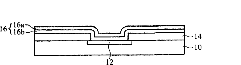
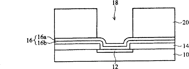
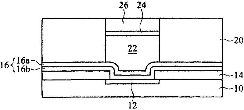
[0031] The present disclosure provides an embodiment of a formation process of a sidewall protection layer for copper pillar bump technology. As used throughout this disclosure, the term "copper pillar bump" refers to a bump structure that includes a conductive copper pillar (pillar or standoff) that includes copper or a copper alloy. Copper pillar bumps can be applied directly to electrical pads, redistribution layers on semiconductor chips for flip-chip assemblies, or other similar applications. In the following description, numerous specific details are set forth to help a more thorough understanding of the present disclosure. However, one of ordinary skill in the art will recognize that the present disclosure may be practiced without these specific details. In some instances, well-known structures and processes have not been described in detail to avoid unnecessarily obscuring the present disclosure. In references throughout the specification, "one embodiment" or "an emb...


PUM


Abstract

An integrated circuit device includes a Cu pillar and a solder layer overlying the Cu pillar. A Co-containing metallization layer is formed to cover the Cu pillar and the solder layer, and then a thermally reflow process is performed to form a solder bump and drive the Co element into the solder bump. Next, an oxidation process is performed to form a cobalt oxide layer on the sidewall surface of the Cu pillar.

Description

[0001] cross reference [0002] This application claims priority to US Provisional Patent Application No. 61 / 394,038, filed October 18, 2010, which is hereby incorporated by reference. [0003] This application is a co-pending application related to US Patent Application No. 12 / 843,760, filed July 26, 2010, which is hereby incorporated by reference. technical field [0004] The present disclosure relates to integrated circuit fabrication and, more particularly, to copper pillar bump structures in integrated circuit devices. Background technique [0005] Flip-chip packaging utilizes bumps to establish electrical contact between the input / output (I / O) pads of the chip and the substrate or leadframe of the package. Structurally, the bump structure includes a bump and a so-called under-bump metallurgy (UBM) between the bump and the I / O pad. A UBM usually includes a bonding layer, a barrier layer, and a wetting layer, which are arranged in this order on the I / O pad. Based on t...

Claims


Application Information

Patent Timeline
IPC IPC(8): H01L23/488H01L21/60
CPCH01L2224/03831H01L2924/01049H01L2224/16227H01L2224/13139H01L2224/13083H01L2224/13164H01L2224/11823H01L24/11H01L2224/13144H01L24/05H01L2924/01078H01L2224/13565H01L24/16H01L2224/1357H01L2224/05666H01L2224/13155H01L24/13H01L2224/11825H01L2224/05144H01L2924/01024H01L2224/13657H01L2224/11622H01L2224/13147H01L2924/01013H01L2924/01322H01L24/03H01L2224/0345H01L2924/01012H01L2224/16225H01L2224/13111H01L2924/01051H01L2224/11464H01L2224/11462H01L2224/81447H01L2924/01327H01L2224/11849H01L2224/1145H01L2924/01047H01L2924/01006H01L2224/81815H01L2924/01079H01L2924/01073H01L2924/01038H01L2224/11452H01L2924/0103H01L2924/01082H01L2924/13091H01L2924/0104H01L2224/13582H01L2924/014H01L2224/13583H01L2924/01023H01L2224/81193H01L2224/0401H01L2924/01029H01L2224/16145H01L2225/06513H01L2924/01019H01L2924/01033H01L2924/01075H01L24/81H01L2224/1308H01L2224/16237H01L2924/1305H01L2924/1306H01L2924/14H01L2924/00H01L23/562H01L2224/13157H01L2924/01027H01L2924/01028H01L2924/0539H01L2924/20102H01L2924/2075H01L2924/20751
Inventor 黄见翎林正怡刘重希
Owner TAIWAN SEMICON MFG CO LTD
Why Eureka
Try Eureka