Radio frequency noise de-embedding method

A technology of radio frequency noise and de-embedding, applied in the direction of electrical components, single semiconductor device testing, electric solid-state devices, etc., can solve problems such as spending more time, wasting silicon chip area, and troublesome testing, so as to reduce testing time and improve Test efficiency, cost reduction effects

A technology of radio frequency noise and de-embedding, applied in the direction of electrical components, single semiconductor device testing, electric solid-state devices, etc., can solve problems such as spending more time, wasting silicon chip area, and troublesome testing, so as to reduce testing time and improve Test efficiency, cost reduction effects

CN102466773AActive Publication Date: 2012-05-23SHANGHAI HUAHONG GRACE SEMICON MFG CORP

Image

  • Radio frequency noise de-embedding method
  • Radio frequency noise de-embedding method
  • Radio frequency noise de-embedding method

Examples


Embodiment Construction

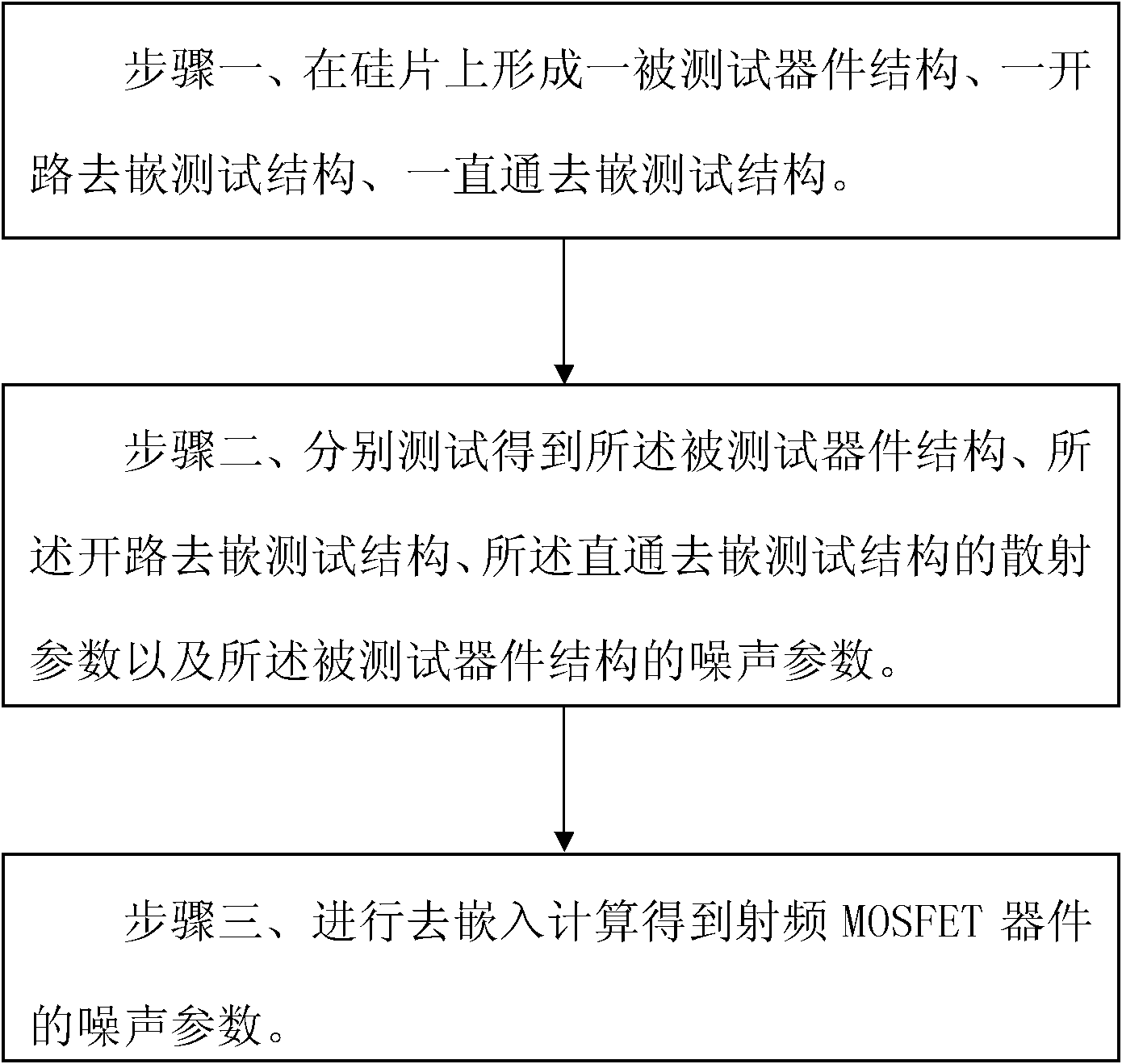
[0038] Such as image 3 As shown, it is a schematic flow chart of the open-through de-embedding method according to the embodiment of the present invention; the open-through de-embedding method according to the embodiment of the present invention includes the following steps:

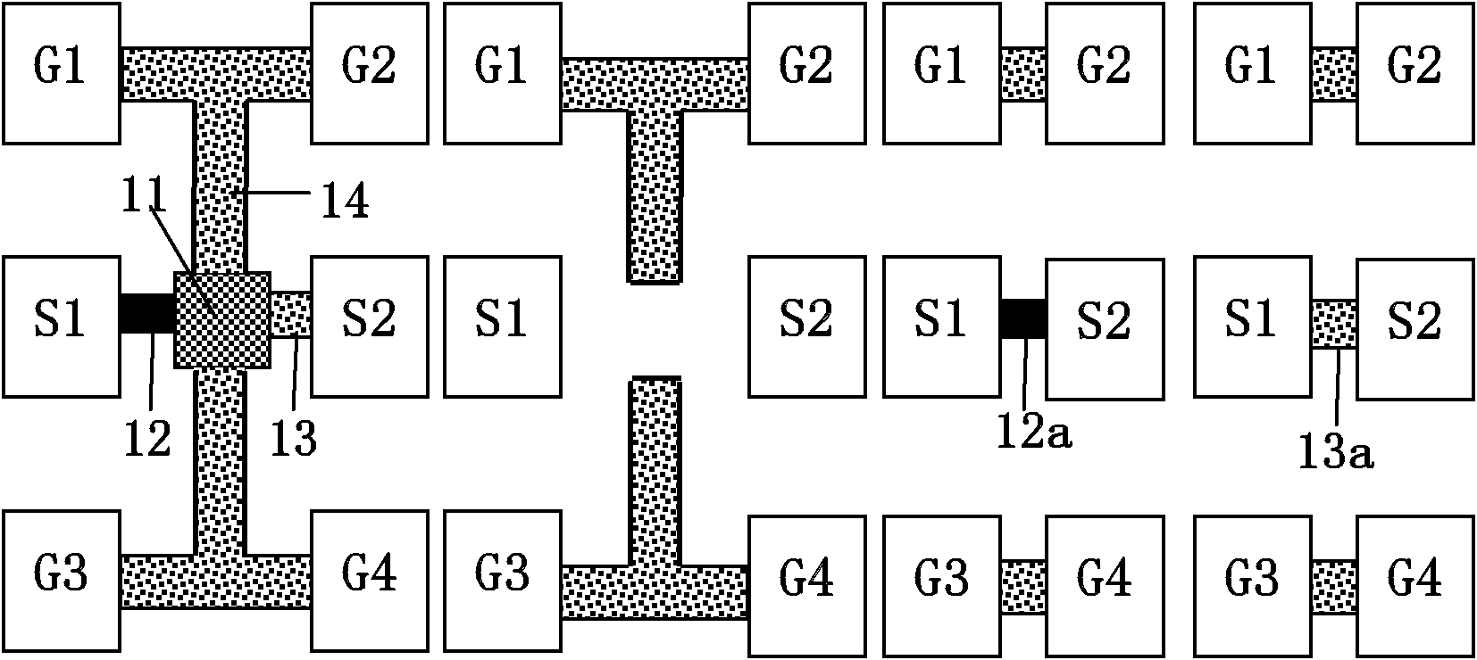
[0039] Step 1, such as Figure 4 As shown, a device under test structure 1, an open circuit de-embedding test structure 2, and a straight-through de-embedding test structure 3C are formed on a silicon chip; the device under test structure 1 includes a radio frequency device 11, a signal input pad S1, a signal output pad S2, four ground pads, the signal input pad S1 is connected to the input end of the radio frequency device 11 through a metal wire 12, the signal output pad S2 and The output terminal of the radio frequency device 11 is connected through the metal wire 2 13, and the four ground pads are connected to each other through the metal wire 3 14 and connected to the ground terminal of the radio ...


PUM


Abstract

The invention discloses a radio frequency noise de-embedding method, which comprises the following steps of: forming a device under test, an open de-embedding test structure and a thru de-embedding test structure on a silicon chip; performing tests to obtain scattering parameters of the device under test, the open de-embedding test structure and the thru de-embedding test structure and a noise parameter of the device under test; and performing de-embedding calculation by utilizing each scattering parameter and the noise parameter of the device under test to obtain a noise parameter of a radio frequency device, wherein the normalized characteristic impedance and propagation constant of a pure metal wire are calculated by utilizing the scattering parameters of inter-signal metal wires of the thru de-embedding test structure, and then an ABCD parameter of an input end metal wire or an output end metal wire of the device under test is calculated. By the method, the number of the thru de-embedding test structures on the silicon chip can be greatly decreased, the area of the silicon chip can be saved, test time can be shortened, and cost can be greatly decreased.

Description

technical field [0001] The invention relates to the field of semiconductor integrated circuit manufacturing, in particular to a radio frequency noise de-embedding method. Background technique [0002] For RF noise testing, the parasitic resistance, capacitance, and inductance of pads and wiring in the test structure will have a relatively large impact on the test results. In order to obtain accurate noise parameters of the device under test (DUT) structure (Device Under Test, DUT), these parasitic effects need to be removed, that is, de-embedding (De-embedding) is required. The most used in the prior art is as described in the document "C.H.CHEN and M.J.DEEN, "High frequency Noise of Mosfets I Modeling". Solid-state Electronics Vol.42, No.11, pp.2069-2081, 1998" The Open de-embedding (Open de-embedding) method; and such as the literature "K.Aufinger and J.Bock, "A Straightforward Noise De-embedding Method and Its Application to High-Speed ​​Silicon Bipolar Transistors", Pro...

Claims


Application Information

Patent Timeline
23 May 2012
Publication
CN102466773A
IPC
G01R31/26; H01L23/544; H01L21/66
CPC
H01L2924/0002; H01L2924/00
Inventors
ι»„ζ™―δΈ°