Active matrix substrate and active matrix display device
An active matrix and substrate technology, which is applied in the field of active matrix display devices, can solve problems such as abnormal line width, poor display, poor wire breakage, etc., and achieve the effect of improving patterning accuracy
- Summary
- Abstract
- Description
- Claims
- Application Information
AI Technical Summary
Problems solved by technology
Method used
Image

Examples
Embodiment approach 1
[0074] Below, according to Figure 1 to Figure 7 The configuration of the TFT array substrate 1 as an active matrix substrate included in a liquid crystal display device which is an example of the active matrix display device of the present invention will be described.
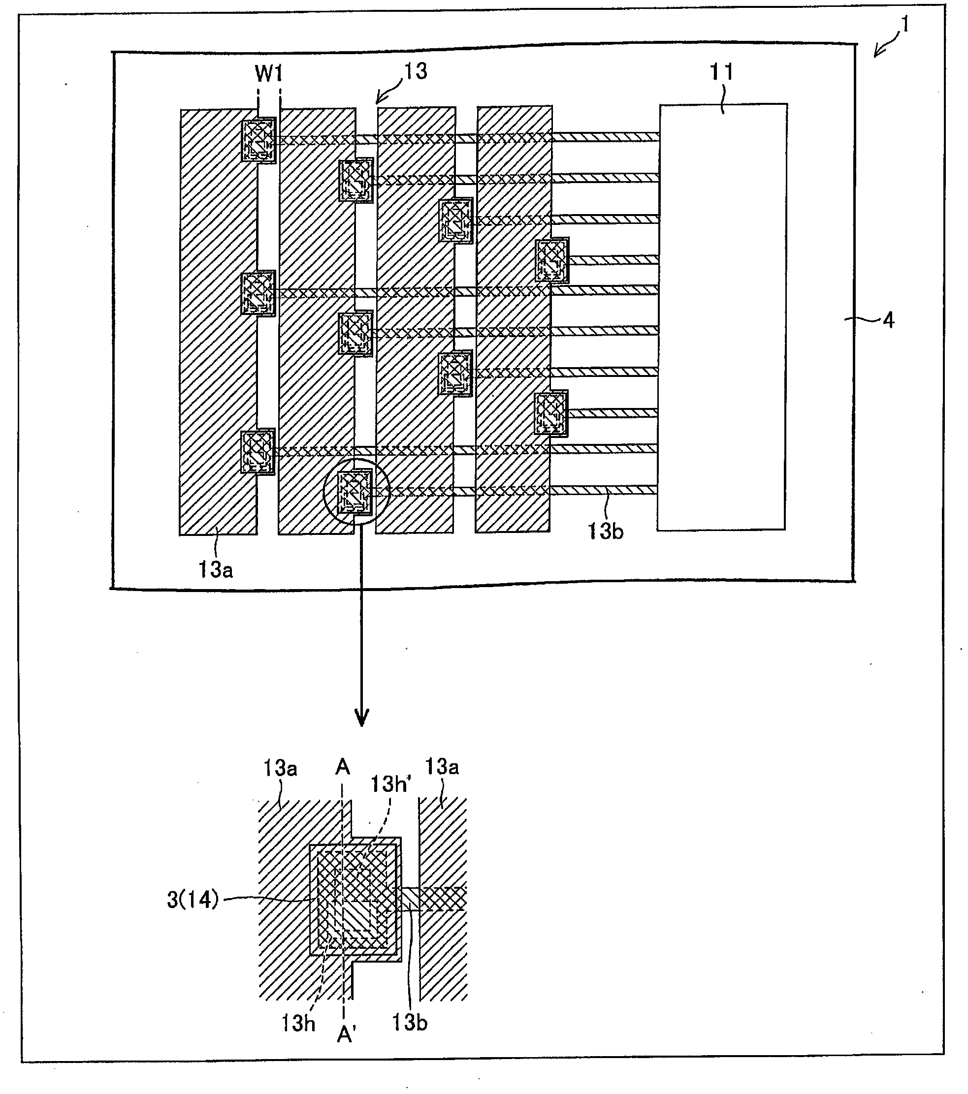
[0075] Figure 4 It is a diagram showing a schematic configuration of the TFT array substrate 1 .
[0076] As shown in the figure, the TFT array substrate 1 includes a display region R1 and a peripheral region R2 located around the display region R1.
[0077] In the display region R1 , pixel TFT elements 2 , and pixel electrodes 3 connected to the pixel TFT elements 2 are provided in a matrix.
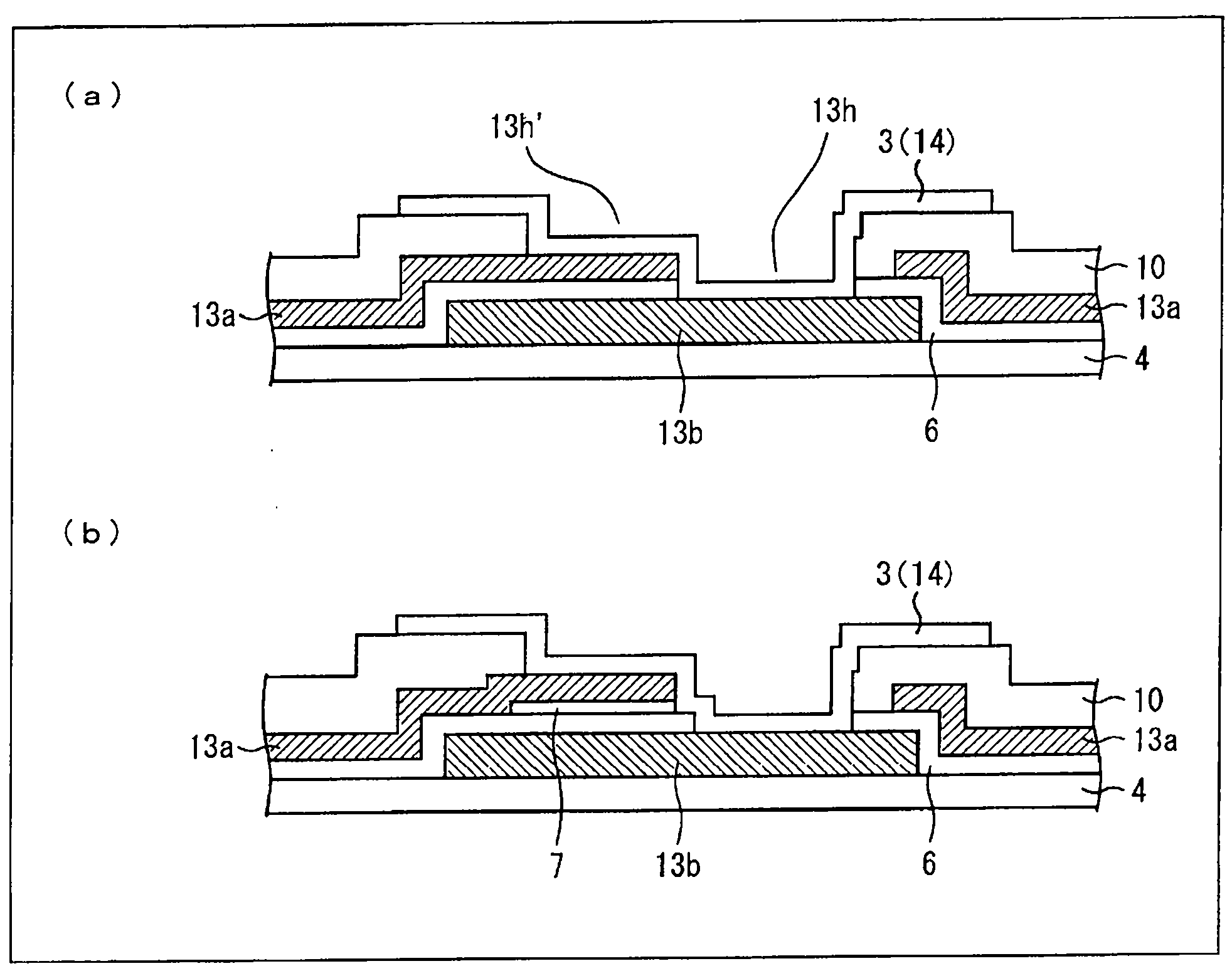
[0078] Such as Figure 4 As shown, the pixel TFT element 2 has the following structure: on the insulating substrate 4, the gate bus line GL and the gate electrode layer 5 are stacked in this order; the gate insulating film 6; the amorphous silicon film 7, which is a semiconductor film; the source Pole, drain electr...
Deformed example 1
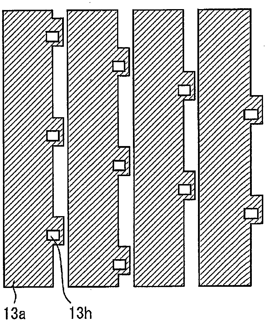
[0130] Figure 5 It is a figure which shows the modification of the patterned shape of the stem wiring 13a.
[0131] Although not shown in the figure, it is preferable that the trunk lines 13a are formed in parallel straight lines with equal width and equal pitch.
[0132] In addition, the structure is such that the region where the main line 13a is connected to the branch line 13b is arranged in a lower layer of the main line 13a.
[0133] According to the above configuration, the interval W2 between the trunk lines 13a can be further reduced, and the increase in the peripheral region R2 where the signal line 13 for a gate drive circuit is formed can be further suppressed.
[0134] In addition, when a sealing material of the type cured by irradiating UV from the back surface of the TFT array substrate 1 is provided on the formation area of the signal wiring 13 for the gate drive circuit, the above-mentioned equal width and equal intervals are formed as parallel straight li...
Deformed example 2
[0137] Figure 6 It is a figure which shows still another modification example of the main wiring 13a and the branch wiring 13b.
[0138] Such as Figure 6 As shown, it is preferable to provide a plurality of trunk wirings 13a, and the trunk wiring 13a disposed farthest from the gate driving circuit 11 among the trunk wirings 13a is located farther from the gate driving circuit 11. position, a second trunk line 15 is provided, and the second trunk line 15 and the second branch line 15a connecting the second trunk line 15 and the gate drive circuit 11 are formed in the same layer as the branch line 13b. The branch line 13 b is the same layer as the gate bus line GL and the gate electrode layer 5 .
[0139] The second main line 15 and the second branch line 15a do not intersect with the branch line 13b which is formed in the same layer as the gate electrode layer 5 in terms of their arrangement, so they can be connected with the branch line 15a. 13b, which is formed in the sa...
PUM
| Property | Measurement | Unit |
|---|---|---|
| thickness | aaaaa | aaaaa |
| thickness | aaaaa | aaaaa |
Abstract
Description
Claims
Application Information
 - R&D
- Intellectual Property
- Life Sciences
- Materials
- Tech Scout
- Unparalleled Data Quality
- Higher Quality Content
- 60% Fewer Hallucinations
Browse by: Latest US Patents, China's latest patents, Technical Efficacy Thesaurus, Application Domain, Technology Topic, Popular Technical Reports.
© 2025 PatSnap. All rights reserved.Legal|Privacy policy|Modern Slavery Act Transparency Statement|Sitemap|About US| Contact US: help@patsnap.com