Electrostatic attracting structure and fabricating method therefor
An electrostatic adsorption and structure technology, which is applied in the manufacture of semiconductor/solid-state devices, holding devices using electrostatic attraction, and manufacturing tools, etc., which can solve the problems of overall complicated work and increased cost.
- Summary
- Abstract
- Description
- Claims
- Application Information
AI Technical Summary
Problems solved by technology
Method used
Image

Examples
Embodiment 1
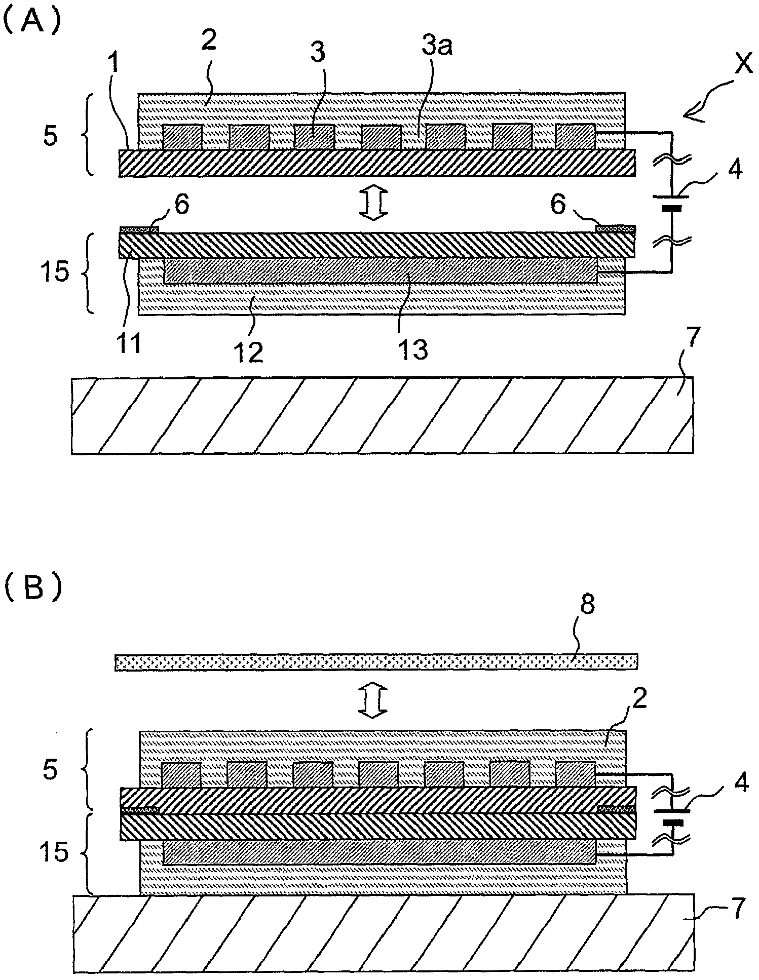
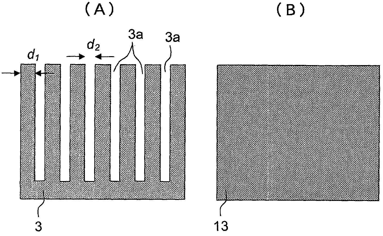
[0031] in figure 1 as well as figure 2 Here, an electrostatic chuck device using the electrostatic adsorption structure X of Example 1 of the present invention as a means for adsorbing and holding a semiconductor substrate such as a silicon wafer by a semiconductor manufacturing process such as plasma etching is shown.
[0032] In the electrostatic chuck device of the first embodiment, the electrostatic adsorption structure X as the adsorption / holding unit of the semiconductor substrate has the sheet members 5 and 15 and the adsorption power source 4, and is equipped with a pipe (not shown) through which a cooling medium flows. A base body 7 made of aluminum, etc., is integrally formed to constitute an electrostatic chuck device, and the dielectric body 2 of the sheet member 5 in the electro-adsorption structure X is used as an adsorption surface to adsorb and hold a semiconductor substrate 8 such as a silicon wafer.
[0033] Here, the surface of the dielectric 1 made of a polyimid...
Embodiment 2
[0038] in Figure 3 ~ Figure 5 In the figure, a display / disclosure device using the electrostatic adsorption structure X of Example 2 of the present invention as a display unit for display / disclosure is shown.
[0039] In the display / revelation device of the second embodiment, the electrostatic adsorption structure X as the above-mentioned display unit has sheet members 25 and 35 and a suction power source 14, so that the dielectric 32 side of the sheet member 35 can be attracted to, for example, the wall surface 10. The disclosure 9 made of a sheet made of paper or resin is attracted to the dielectric 22 side of the sheet member 25.
[0040] Here, a PET film (dielectric) 21 having a size of 400 mm in length × 600 mm in width × 50 μm in thickness is screen-printed with carbon ink (JELCON type CH-10 manufactured by Jujo Chemical Co., Ltd.) to form 350 mm in length × 550 mm in width. × an electrode 23 with a thickness of 10 μm, and then screen printing an insulating ink (JELCON type...
Embodiment 3
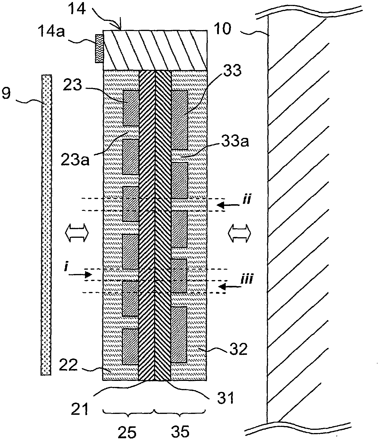
[0047] in Image 6 Here, a modification example of the electrostatic adsorption structure X used in the above-mentioned Example 2 is shown. Using two sheet members 25 on which the electrostatic adsorption structure X in Example 2 was formed, a sheet member 45 was further placed between them, and three sheet members were laminated to form the electrostatic adsorption structure of Example 3 X. Among them, the sheet member 45 is formed in the same manner as the sheet member 25 except that the entire surface of the sheet member 45 is provided with an electrode 43 of 350 mm in length × 550 mm in width × 10 μm in thickness, without forming an opening. In addition, in the electrostatic adsorption structure X of Example 3, two adsorption power sources 14 are used to apply a voltage between the electrodes of opposing sheet members, and it is formed in the same manner as in Example 2 except for that.
[0048] In addition, in the electrostatic adsorption structure X of the third embodiment...
PUM
| Property | Measurement | Unit |
|---|---|---|
| thickness | aaaaa | aaaaa |
| thickness | aaaaa | aaaaa |
Abstract
Description
Claims
Application Information
 - R&D
- Intellectual Property
- Life Sciences
- Materials
- Tech Scout
- Unparalleled Data Quality
- Higher Quality Content
- 60% Fewer Hallucinations
Browse by: Latest US Patents, China's latest patents, Technical Efficacy Thesaurus, Application Domain, Technology Topic, Popular Technical Reports.
© 2025 PatSnap. All rights reserved.Legal|Privacy policy|Modern Slavery Act Transparency Statement|Sitemap|About US| Contact US: help@patsnap.com