Laser beam coupling output device for high-power semiconductor

A laser beam, coupled output technology, applied in the direction of optics, optical components, instruments, etc., can solve the problems of increasing the difficulty of machining laser parts, affecting the quality of the output beam beam, increasing the cost of the laser system, etc., to reduce the difficulty of machining , reduced volume and weight, and reasonable structure

Inactive Publication Date: 2011-04-13
BEIJING UNIV OF TECH
View PDF4 Cites 21 Cited by
  • Summary
  • Abstract
  • Description
  • Claims
  • Application Information

AI Technical Summary

Problems solved by technology

Although this method can obtain high-power laser output, the beam quality of the output beam is affected to a certain extent because no beam shaping device is added and the optical paths of the two paths of light passing through the polarization coupler are different.
[0004] Patent No. 200910076298.3 provides a beam recombination device, although it solves the problems

Method used


Image

  • Laser beam coupling output device for high-power semiconductor
  • Laser beam coupling output device for high-power semiconductor
  • Laser beam coupling output device for high-power semiconductor

Examples


Embodiment 1

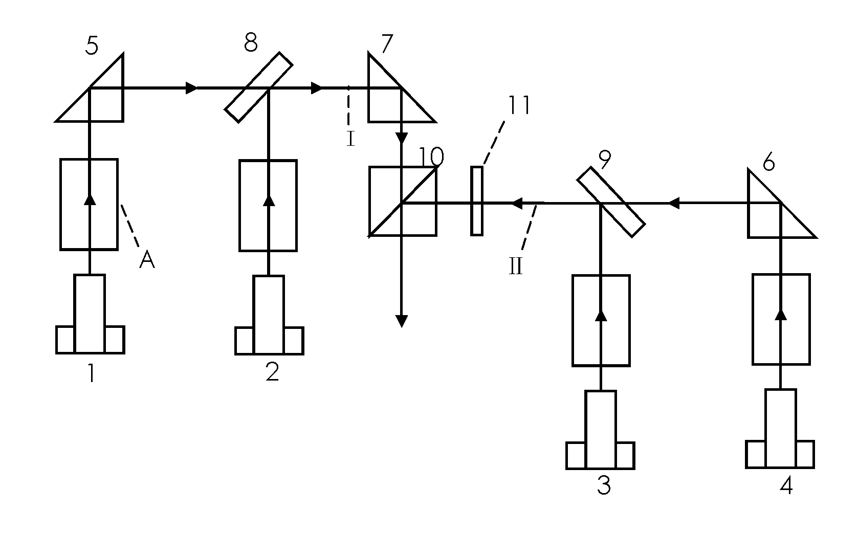
[0031] Such as figure 1 As shown, a high-power semiconductor laser beam coupling output device consists of the first semiconductor laser array 1, the second semiconductor laser array 2, the third semiconductor laser array 3, the fourth semiconductor laser array 4, the first rectangular prism 5, the second A rectangular prism 6, a third rectangular prism 7, a first wavelength coupler 8, a second wavelength coupler 9, a polarization coupler 10, a half-wave plate 11 and four shaping devices A. The four shaping devices A are respectively located behind the four semiconductor laser arrays, and the half-wave plate 11 is placed between the second wavelength coupler 9 and the polarization coupler 10 perpendicular to the propagation direction of the optical path. The surfaces of the first rectangular prism 5 , the second rectangular prism 6 , and the third rectangular prism 7 are coated. The first wavelength coupler 8 and the second wavelength coupler 9 are spectroscopic elements such ...

Embodiment 2

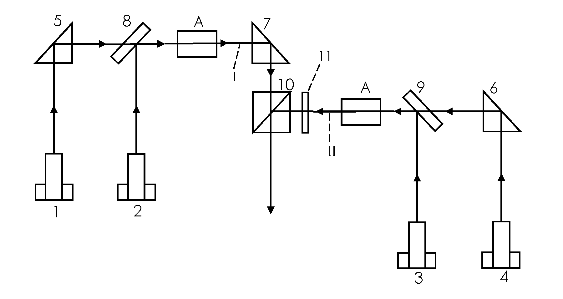
[0035] Such as figure 2 As shown, the difference between embodiment 2 and embodiment 1 is that the light emitted by the semiconductor laser array in embodiment 2 is firstly subjected to wavelength coupling, and then undergoes beam shaping. That is, the four beam shaping devices located behind the semiconductor laser array are canceled, and only two beam shaping devices are placed after the first wavelength coupler 8 and after the second wavelength coupler 9 .

Embodiment 3

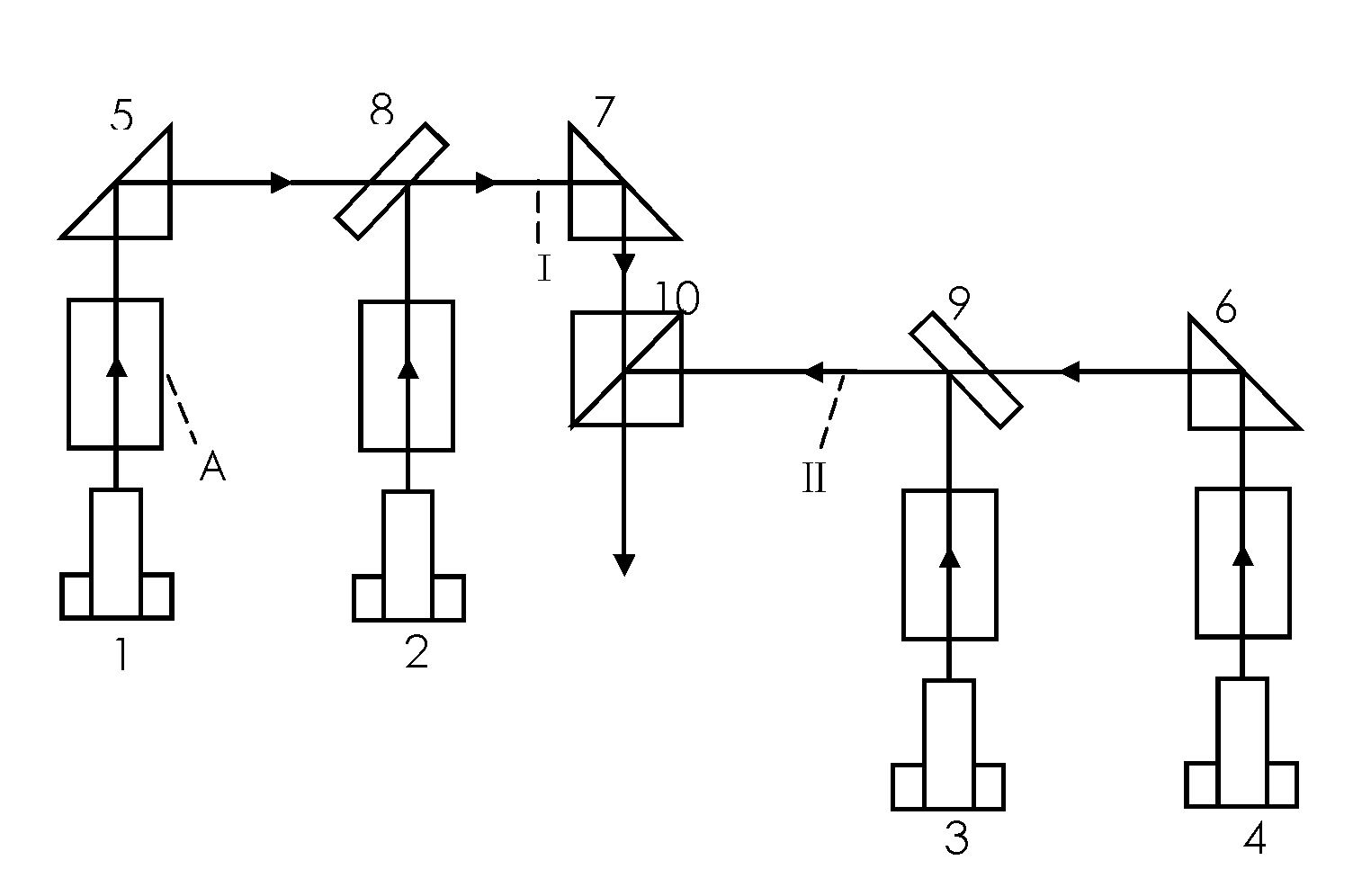
[0037] Such as image 3 As shown, a high-power semiconductor laser beam coupling output device consists of the first semiconductor laser array 1, the second semiconductor laser array 2, the third semiconductor laser array 3, the fourth semiconductor laser array 4, the first rectangular prism 5, the second A rectangular prism 6, a third rectangular prism 7, a first wavelength coupler 8, a second wavelength coupler 9, a polarization coupler 10 and four shaping devices A. The four shaping devices A are respectively located behind the four semiconductor laser arrays. The surfaces of the first rectangular prism 5 , the second rectangular prism 6 , and the third rectangular prism 7 are coated. The first wavelength coupler 8 and the second wavelength coupler 9 are spectroscopic elements such as prisms, gratings, and interferometers. The polarizing coupler 10 is a Glan-Taylor prism, a thin-film polarizing device, a film with polarizing effect or a natural birefringent crystal.

[00...


PUM


Abstract

The invention relates to a multi-beam coupling output device for a high-power semiconductor laser system, belonging to the technical field of laser. With respect to the device, light with two wavelengths, which is respectively emitted by a first semiconductor laser array and a second semiconductor laser array, is subject to wavelength coupling by using a wavelength coupler, thus obtaining a beam with two wavelengths; light with two wavelengths, which is respectively emitted by a third semiconductor laser array and a fourth semiconductor laser array, is subject to wavelength coupling by using the wavelength coupler, thus obtaining a beam comprising two wavelengths; and the two beams respectively with two wavelengths are combined by a polarization coupler to finally obtain a combined beam, and the combined beam is output. The coupling output device has more reasonable structure, smaller volume, good controllability and lower cost, and is easy to process.

Description

technical field [0001] The invention relates to a multi-beam coupling output device in a high-power semiconductor laser system. The device uses a method of combining wavelength coupling and polarization coupling to combine beams of two wavelengths emitted by four groups of semiconductor laser arrays into one beam, belonging to laser optoelectronics and its fields of application. Background technique [0002] High-power semiconductor lasers are widely used in material processing, military, medical and other fields due to their advantages such as small size, high photoelectric conversion rate, and long life, especially kilowatt-level high-power semiconductor lasers with high beam quality and high brightness are more widely used . [0003] At present, in order to realize high-power semiconductor laser output in the world, the commonly used methods include spatial multi-channel coupling method, polarization coupling method and wavelength coupling method. For example, JENOPTIK ...

Claims


Application Information

Patent Timeline
IPC IPC(8): G02B27/28G02B27/10G02B27/09G02B5/30
Inventor 王智勇高静曹银花刘友强
Owner BEIJING UNIV OF TECH
Why Eureka
Try Eureka