Light emission apparatus

a technology of light emission apparatus and light source, which is applied in the direction of lighting and heating apparatus, fixed installation, lighting support devices, etc., can solve the problems of resin general deterioration, high light intensity, and prominent deterioration of resin, and achieve a reasonable structure suitable for practical use.

Active Publication Date: 2006-09-05
SIGNIFY HLDG BV
View PDF8 Cites 57 Cited by
  • Summary
  • Abstract
  • Description
  • Claims
  • Application Information

AI Technical Summary

Benefits of technology

[0011]The object of the present invention is to provide a light emission apparatus suitable for a high-intensity surface light-source, and having a reasonable structure suitable for practical use.
[0013]With the stated construction, the area of the insulation film, which is not a light emitting surface (i.e. a surface area of the insulation film which is exposed), is provided with a light reflective layer for reflecting alight that deteriorates resin. Therefore, it becomes possible to reduce the amount of light that the light emission chip irradiates through the light reflective layer towards the insulation film, thereby restricting deterioration of the insulation film. In addition, the light reflective layer is provided to cover the side surface of the light emission chip, and so the heat emitted from the light emission chip through the side surface thereof is facilitated to be dissipated towards the insulation film. Accordingly, with the surface emission type light source, too, a favorable heat dissipation characteristic is assured, thereby realizing a light emission apparatus having reasonable structure suitable for practical use.
[0017]In addition, if the light emission chip that emits excitation light is either a resonant light emitting diode chip or a vertical-cavity surface-emitting laser chip, then the light emitted in vertical direction from the light emission surface of the light emission chip will be directly irradiated on the phosphor layer, without dispersing, thereby improving the light emission efficiency of the light emission apparatus.
[0018]Note that a thread hole and a groove may be provided with respect to the substrate in a position where the light emission chip is provided in a plan view, the thread hole being to be used in mounting of the light emission apparatus, the groove being to absorb distortion which occurs when the substrate expands due to heat. According to this construction, if the light emission apparatus is fixed by means of screws, the chips will be prevented from falling off, as a result of the distortion of the substrate due to thermal expansion.
[0020]Furthermore, the light emission chip may be made to abut against the phosphor layer. With such a structure, the thickness of the light emission apparatus can be made thinner, thereby realizing more compact structure therefor.

Problems solved by technology

Incidentally, the resin generally deteriorates because the atom coupling is cut by means of the energy that the light has.
In particular, the excitation light has a high energy, and so the deterioration in resin is prominent.
The resin is easy to deteriorate by means of the excitation light, and so turns yellow thereby changing light-emitting color, or cracks which then incurs entry of water, thereby deactivating the phosphor particles from the entered water, or increasing leak current in a case where the water adheres to the surface of the LED chips.
In addition, the shell-type white LEDs are so-called discrete parts that emit white light independently from one another, therefore have limitation in enhancing mounting density, and incur large cost.
In spite of these advantages, however, the hybrid structure is expected to have a problem that, since all the excitation light emitted from the LED chips will not be converted into visible light by the phosphor film, a part of the excitation light will be reflected on the resin covering the insulating substrate, to deteriorate the resin.
However, because of being expensive, the ceramic substrate is not suitable for this use if it requires numerous chips and so requires a large area.
However, there is a limitation in preventing the excitation light from reflection.
In addition, new problems are considered to arise.

Method used


Image

  • Light emission apparatus
  • Light emission apparatus
  • Light emission apparatus

Examples


first embodiment

(The First Embodiment)

[0039](1) The Entire Structure of Illumination Apparatus

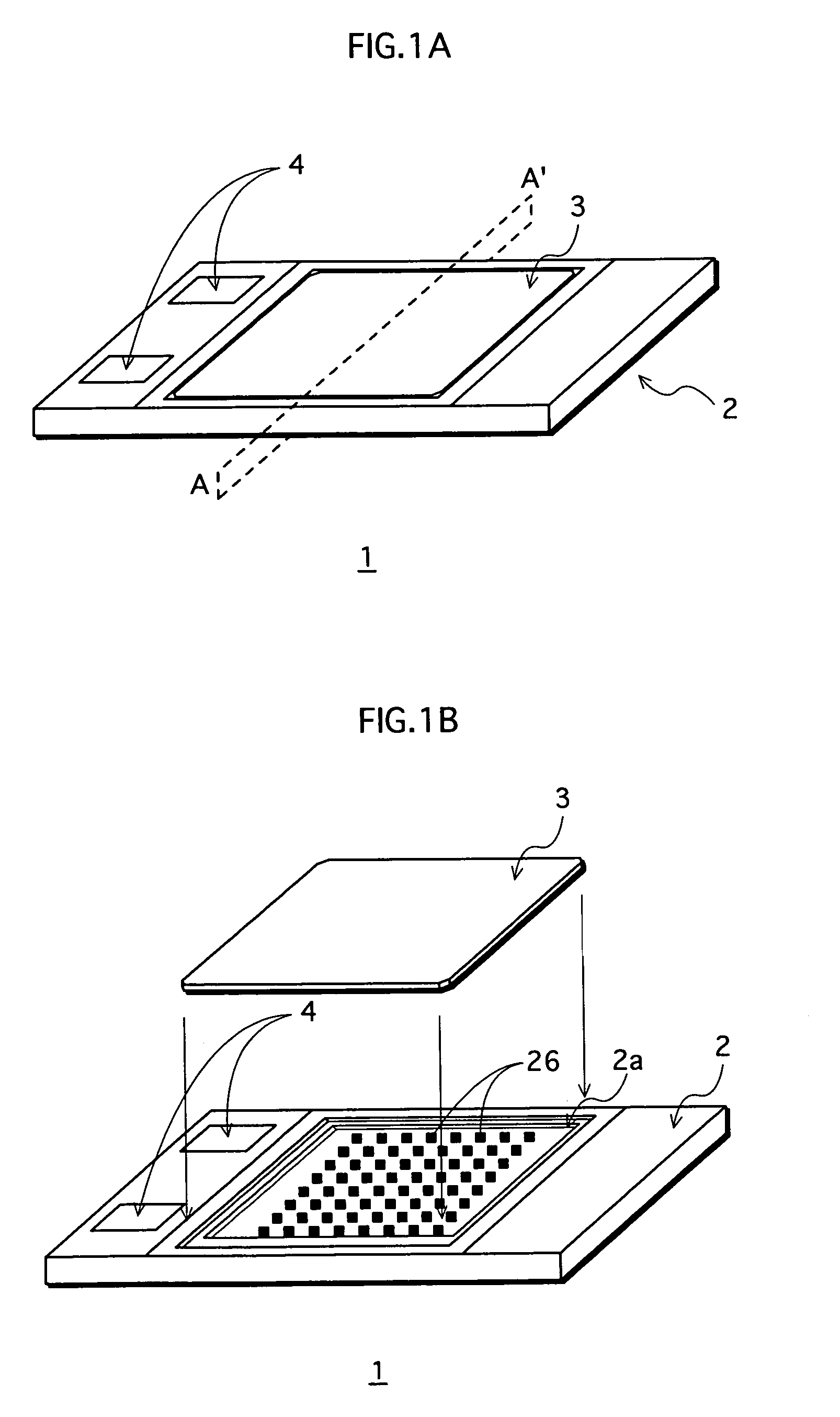
[0040]FIG. 1A is a schematic slanting view of the illumination apparatus that relates to the first embodiment of the present invention, and FIG. 1B is an exploded slanting view of the illumination apparatus.

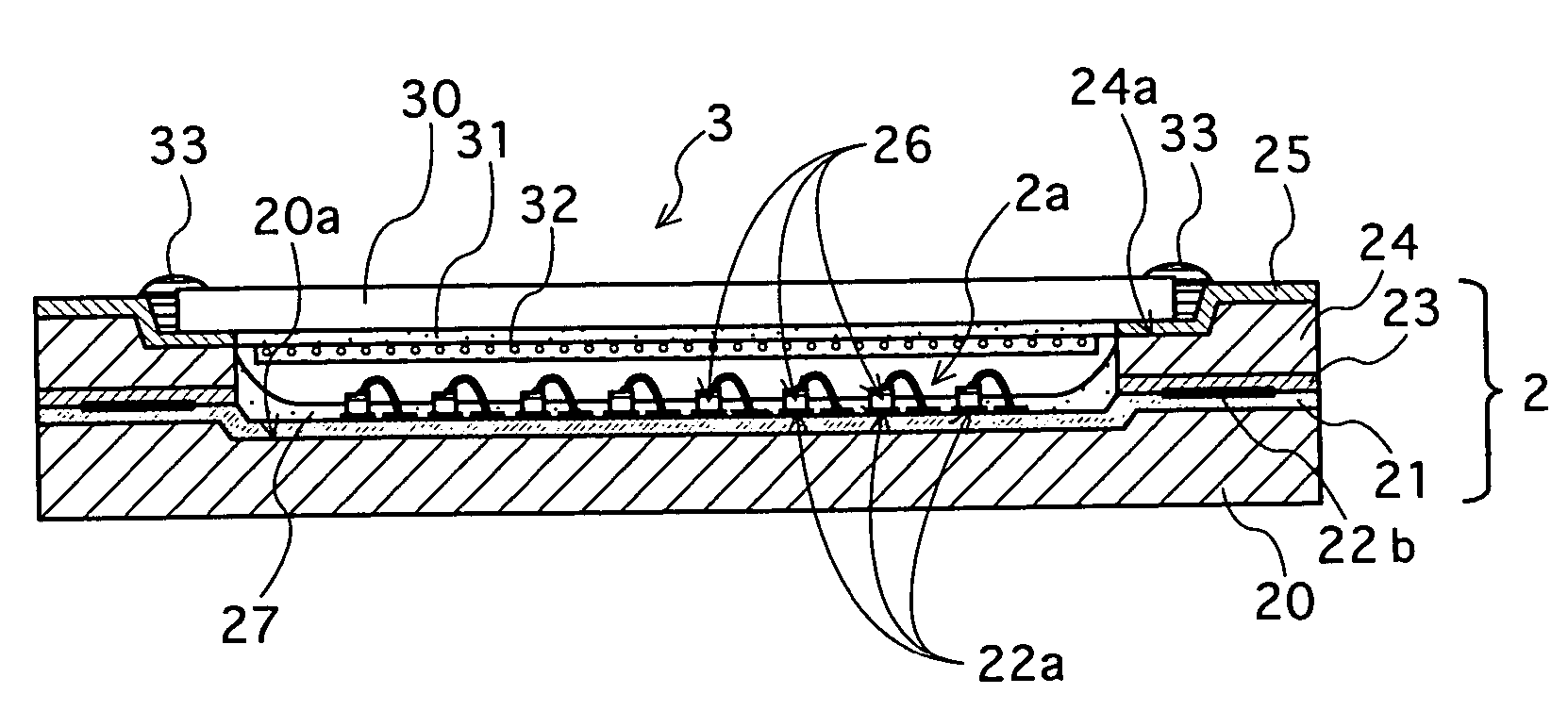
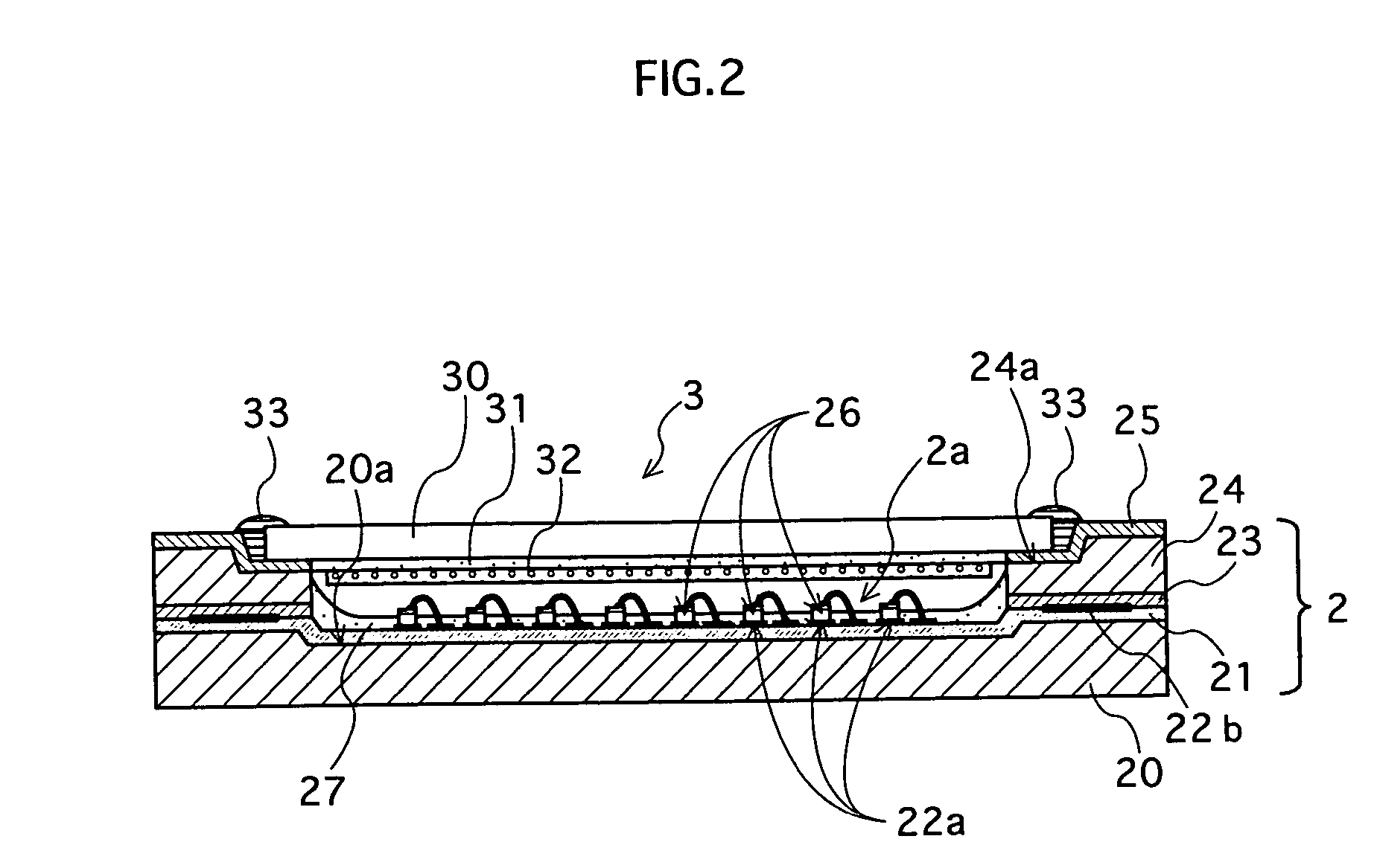
[0041]As shown in these drawings, the illumination apparatus 1 is comprised of a substrate section 2, a cover 3, and a power-feeder 4. The substrate section 2 is flat-shaped and has a concave 2a in the middle thereof. At the bottom of the concave 2a, a plurality of chips 26 are arranged in a grid pattern. The chips 26 are hermetically sealed, by the structure in which the cover 3 that is also flat-shaped is fixed to the substrate section 2 to cover the concave 2a. Furthermore, the upper main surface of the substrate section 2 is provided with the power-feeder 4 for feeding electricity from an outside source to the chips 26.

[0042]FIG. 2 is a sectional view of the illumination apparatus 1 shown in FIG. 1A...

second embodiment

(The Second Embodiment)

[0115]The only difference between the illumination apparatus of the second embodiment and the illumination apparatus of the aforementioned first embodiment lies mainly in mounting method of the cover. Therefore, the same structure as the first embodiment will not be explained in this embodiment.

[0116]FIG. 13A is a slanting view of an illumination apparatus 6 that relates to the second embodiment; and FIG. 13B is a slanting view of the illumination apparatus 6, from which a cover 63 has been removed.

[0117]As shown in these drawings, the illumination apparatus 6 has a substrate section 62, the cover 63, and a power-feeder 64. Just as in the first embodiment, on one main surface of the substrate section 62, a concave 62a is provided, for which chips 626 are provided. The cover 63 is fixed, in a sealed condition, to the opening of the concave 62a, so as to cover the chips 626.

[0118]FIG. 14 is a sectional view of the illumination apparatus 6 which is taken along th...


PUM


Abstract

A light emission apparatus that can restrict deterioration of resin used for the light emission apparatus, and that has a reasonable structure fit for actual use is provided, in which a light reflective layer is provided to cover the side surfaces of the chips 26 provided in the concave 2a. According to this, excitation light reflected by the phosphor layer 32, such as ultraviolet light, is reflected again by the light reflective layer 27. Therefore, the excitation light will not reach the resin layer 21, thereby restraining the deterioration of the resin. Moreover, the light reflective layer 27 covers the side surfaces of the chips 26, thereby efficiently conducting the heat emitted from the chips 26 to the metal substrate 20 via the resin layer 21. This improves the heat-dissipation efficiency of the chips 26.

Description

BACKGROUND OF THE INVENTION[0001](1) Field of the Invention[0002]The present invention relates to a light emission apparatus used as a light source of an illumination apparatus and of a display, and in particular relates to a technology for restricting deterioration in resin materials used in such a light emission apparatus.[0003](2) Related Art[0004]Recently, in the field of illumination apparatuses, LED is getting attention as a light source. This is because with LED, light emitting energy can be expected to be improved in the future by research and development. Moreover, with LED, a surface light source with high intensity can be obtained by mounting a plurality of LEDs.[0005]An example of surface light source using LEDs is disclosed in “Optical display” Ohm MOOK Hikari series No. 2, Ohmsha Ltd., Feb. 25, 2002, p. 46–52. In this document, a plurality of shell-type white LEDs are arranged on a substrate. Here, the shell-type white LED has a structure of molding LED chips emitting ...

Claims


Application Information

Patent Timeline
Patent Type & Authority Patents(United States)
IPC IPC(8): F21V29/00F21V21/00F21S2/00F21S8/04F21V19/00F21Y101/02H01L23/02H01L25/075H01L33/50H01L33/60H01L33/62H01L33/64H01S5/022H01S5/323
CPCF21K9/00F21V19/001F21Y2101/02H01L25/0753H01L2924/01322H01R12/7076H01L2224/45144H01L2224/48091F21Y2105/001H01L33/60H01L2924/00014H01L2924/00F21Y2105/10F21Y2115/10
Inventor NAGAI, HIDEOOSHIO, SHOZOYURI, MASAAKI
Owner SIGNIFY HLDG BV
Why Eureka
Try Eureka