
Photoelectric element

A photoelectric component and photoelectric technology, applied in the direction of electrical components, circuits, semiconductor devices, etc., can solve problems such as poor luminous efficiency of light-emitting diode components 1, and achieve the effect of improving luminous efficiency

Inactive Publication Date: 2012-05-30
CHI MEI LIGHTING TECH +1
View PDF4 Cites 12 Cited by
  • Summary
  • Abstract
  • Description
  • Claims
  • Application Information

AI Technical Summary

Problems solved by technology

When the current flows from the second electrode 17 (positive pole) to the first electrode 16 (negative pole), there will be velocity components along the X, Y, Z axis directions ( figure 1 V only X , V Y speed component), and the carriers will quickly pass through the main light-emitting region, and cannot stay in the main light-emitting region for a long time to effectively recombine and generate photons, thus resulting in poor luminous efficacy of the light-emitting diode element 1

Method used


Image

  • Photoelectric element
  • Photoelectric element
  • Photoelectric element

Examples


Embodiment Construction

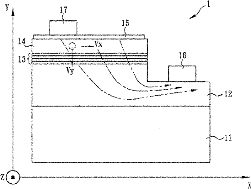
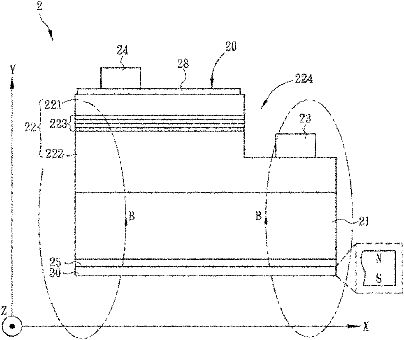
[0034] A photoelectric element according to a preferred embodiment of the present invention will be described below with reference to related drawings, wherein the same elements will be described with the same reference symbols.

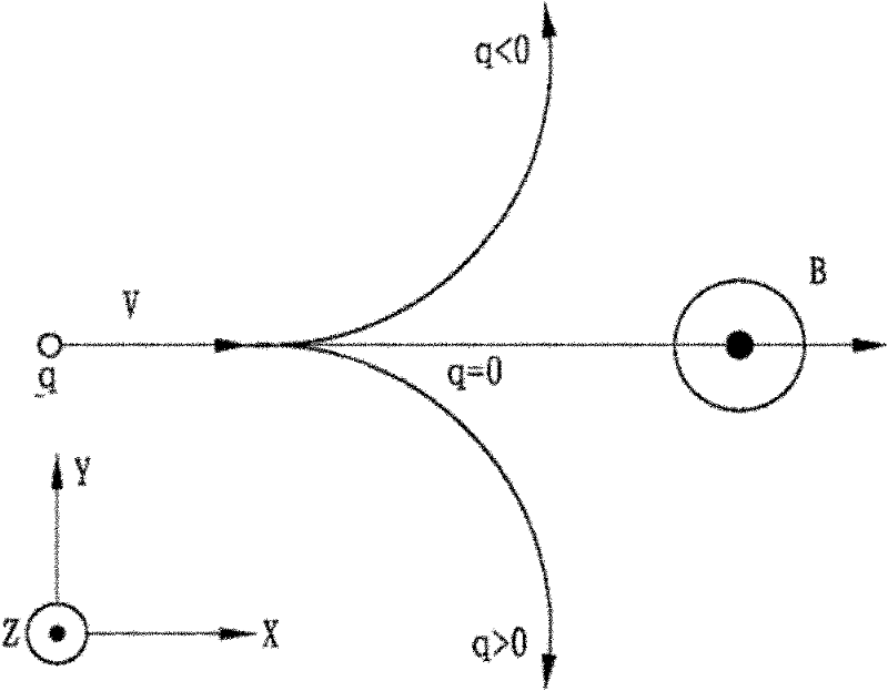
[0035] Before describing the present invention, start with figure 2 Briefly describe the Hall effect. The Hall effect means that when a solid conductor has a current passing through it and is placed in a magnetic field, the charge carriers in the conductor are biased to one side by the Lorentz force, and then a voltage is generated. In addition to the conductor, the semiconductor can also produce the Hall effect. , and the Hall effect of semiconductors is stronger than that of conductors. Such as figure 2 As shown, the carriers move at the speed V in the X-axis direction, and there is another magnetic field B in the movement space of the carriers, and the direction of the magnetic force is the Z-axis direction pointed out on the paper. When the ...


PUM


Abstract

Disclosed is a photoelectric element, composed of a photoelectric lamination layer and a magnetic member, wherein the magnetic member is arranged inside or adjacent to the photoelectric lamination layer and generates a magnetic field to pass through the photoelectric lamination layer. The magnetic member generates a magnetic field penetrating the photoelectric lamination layer, thereby making the motion charge carriers inside the photoelectric lamination layer change the motion path thanks to the Hall effect and accordingly raise the photoelectric efficiency.

Description

technical field [0001] The present invention relates to a photoelectric element, in particular to a photoelectric element with a magnetic component to generate a magnetic field. Background technique [0002] A light-emitting diode (LED) is a light-emitting element made of semiconductor materials. Since light-emitting diodes belong to cold light, they have the advantages of low power consumption, long life of components, fast response speed, etc., coupled with the characteristics of small size and easy to make extremely small or array components, so in recent years, with the continuous advancement of technology, Its application range covers indicator lights of computers or home appliances, backlights of liquid crystal display devices, and even traffic signs or vehicle indicator lights. [0003] figure 1 It is a schematic side view of a known LED element 1 . The LED element 1 includes a substrate 11 , an N-type semiconductor layer 12 , a multiple quantum well layer 13 , a P...

Claims


Application Information

Patent Timeline
IPC IPC(8): H01L33/14H01L33/00
Inventor 卢宗宏余国辉
Owner CHI MEI LIGHTING TECH
Learn More