Manufacturing method of strain CMOS device

A manufacturing method and device technology, applied in semiconductor/solid-state device manufacturing, electrical components, circuits, etc., can solve the problems of thickness consumption, damage to the first stress layer 101, and small spacing, so as to facilitate removal, solve over-etching, The effect of simple deposition process

Active Publication Date: 2014-03-12
SEMICONDUCTOR MANUFACTURING INTERNATIONAL (BEIJING) CORP
View PDF3 Cites 0 Cited by
  • Summary
  • Abstract
  • Description
  • Claims
  • Application Information

AI Technical Summary

Problems solved by technology

[0010] The existing strained CMOS device manufacturing process has the following problems: with the increasing integration of semiconductor devices, the distance between adjacent gates in CMOS devices is also getting smaller and smaller. Void issue is generated, while ensuring the thickness of the stress layer to provide sufficient stress, in figure 2 In the steps shown, the deposition thickness of the thin film oxide layer 200 needs to be very thin, usually no more than , much smaller than the thickness of the stress layer
Since the thin film oxide layer 200 is too thin relative to the thickness of the second stress layer 102, and the thickness will be further consumed when used as a hard mask, it is easy to stop at the thin film when etching the second stress layer 102. The oxide layer 200 directly penetrates through the thin film oxide layer 200 and damages the first stress layer 101 by overetching. For details, see Figure 8 The area circled in

Method used


Image

  • Manufacturing method of strain CMOS device
  • Manufacturing method of strain CMOS device
  • Manufacturing method of strain CMOS device

Examples


Embodiment Construction

[0031] In order to make the above objects, features and advantages of the present invention more comprehensible, specific implementations of the present invention will be described in detail below in conjunction with the accompanying drawings.

[0032] In the following description, many specific details are set forth in order to fully understand the present invention, but the present invention can also be implemented in other ways than those described here, so the present invention is not limited by the specific embodiments disclosed below.

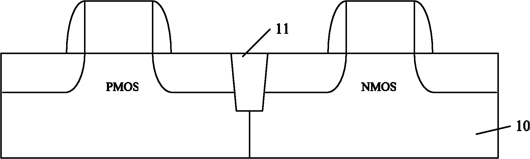
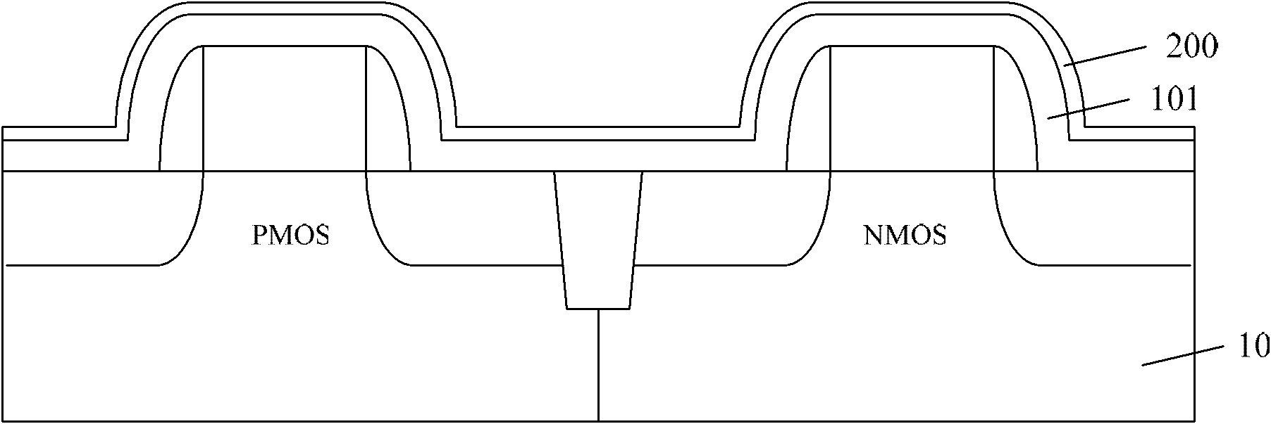
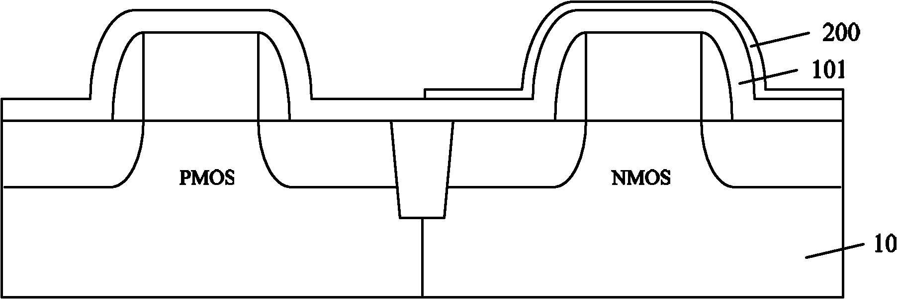
[0033] As mentioned in the background technology section, in the existing strained CMOS device manufacturing method, because the thin film oxide layer is too thin relative to the thickness, over-etching phenomenon is easy to occur during the etching process of the top strained layer, which penetrates and damages the bottom strained layer .

[0034] In view of the above problems, the inventors of the present invention provide a method for ...


PUM


Abstract

The invention provides a manufacturing method of a strain CMOS device. The method comprises the following steps: providing a CMOS device; successively forming a first stress layer and a film oxidation layer on a CMOS device surface; imaging the film oxidation layer so as to expose a part of the first stress layer which is located in a PMOS transistor area; taking the film oxidation layer as a hard mask so as to etch the first stress layer; at least forming a sacrificial barrier layer on a film oxidation layer surface; forming a second stress layer on a formed semiconductor structure surface; taking the sacrificial barrier layer as an etching stop layer so as to etch a part of the second stress layer which is located in the NMOS transistor area; removing the sacrificial barrier layer. In the invention, through forming the sacrificial barrier layer on the film oxidation layer surface and taking the sacrificial barrier layer as the etching stop layer, a problem of over etching can be solved. Further, the sacrificial barrier layer can be amorphous carbon. A deposition technology is simple and the sacrificial barrier layer removing is easy to be performed.

Description

technical field [0001] The invention relates to the technical field of semiconductors, and more specifically, the invention relates to a method for manufacturing a CMOS device using strain technology. Background technique [0002] In semiconductor devices, especially MOS devices, one of the main ways to increase the switching frequency of field effect transistors is to increase the driving current, and the main way to increase the driving current is to increase the carrier mobility. An existing technology for improving the carrier mobility of field effect transistors is strain technology. By forming a stress layer on the surface of the field effect transistor, a stable stress is formed in the channel region of the transistor through the stress layer to improve the carrier mobility in the channel. Among them, tensile stress can make the molecular arrangement in the channel region more loose, thereby improving the mobility of electrons, which is suitable for NMOS transistors; ...

Claims


Application Information

Patent Timeline
Patent Type & Authority Patents(China)
IPC IPC(8): H01L21/336
Inventor 黄敬勇韩秋华张翼英
Owner SEMICONDUCTOR MANUFACTURING INTERNATIONAL (BEIJING) CORP
Why Eureka
Try Eureka