
Electrostatic chuck and plasma device therewith

An electrostatic chuck and plasma technology, applied in the field of microelectronics, can solve the problems of reducing the adsorption force of the wafer, increasing the diameter of the conductive hole, processing difficulties, etc., and achieving the effects of reducing the possibility, reducing the surface contact, and having a simple structure

Active Publication Date: 2012-06-06
BEIJING NAURA MICROELECTRONICS EQUIP CO LTD
View PDF2 Cites 4 Cited by
  • Summary
  • Abstract
  • Description
  • Claims
  • Application Information

AI Technical Summary

Problems solved by technology

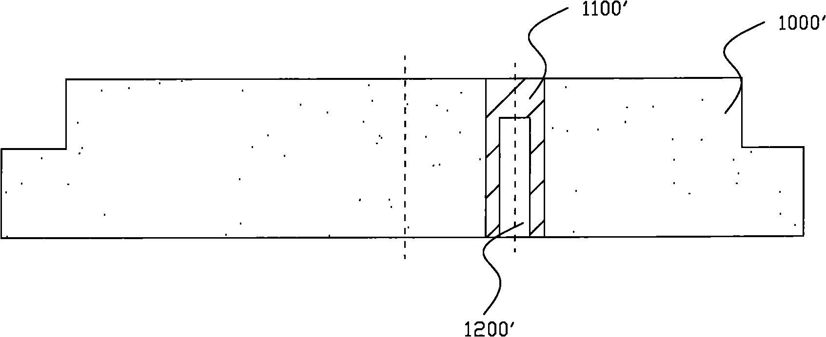
The disadvantage of the prior art is that due to the objective reason that the insulating layer of the conductive hole 1100' and the electrostatic chuck 1000' are made of different materials, the processing is difficult and the cost is high; in addition, if the conductive hole 1100' and the wafer are to be reliably connected contact, it is necessary to increase the diameter of the conductive hole 1100'
However, since the conductive hole 1100' cannot produce an adsorption force on the wafer on the electrostatic chuck 1000', the increase in the diameter of the conductive hole 1100' will significantly reduce the adsorption force of the electrostatic chuck 1000' to the wafer.

Method used


Image

  • Electrostatic chuck and plasma device therewith
  • Electrostatic chuck and plasma device therewith
  • Electrostatic chuck and plasma device therewith

Examples


Embodiment Construction

[0034] Embodiments of the present invention are described in detail below, examples of which are shown in the drawings, wherein the same or similar reference numerals designate the same or similar elements or elements having the same or similar functions throughout. The embodiments described below by referring to the figures are exemplary only for explaining the present invention and should not be construed as limiting the present invention.

[0035] In the description of the present invention, the terms "longitudinal", "transverse", "upper", "lower", "front", "rear", "left", "right", "vertical", "horizontal", " The orientations or positional relationships indicated by "top", "bottom", "inner", "outer", etc. are based on the orientations or positional relationships shown in the drawings, and are only for the convenience of describing the present invention and do not require that the present invention must be constructed in a specific orientation and operation, and therefore sh...


PUM


Abstract

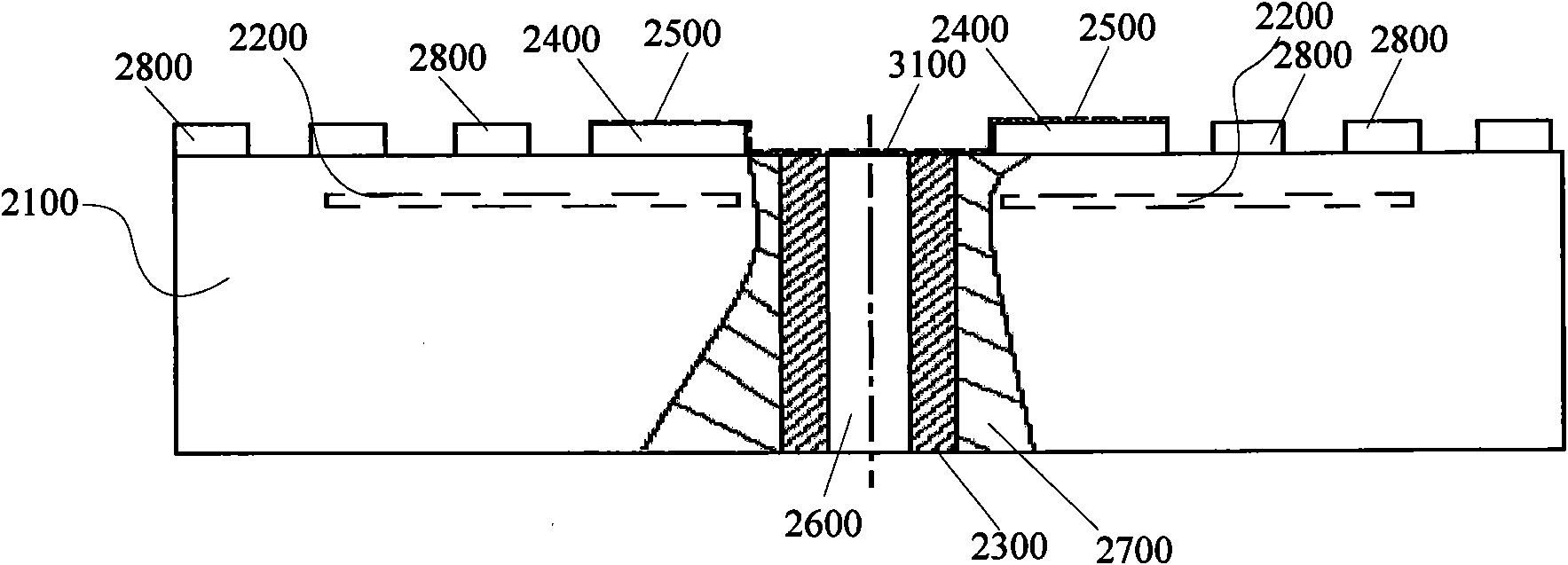
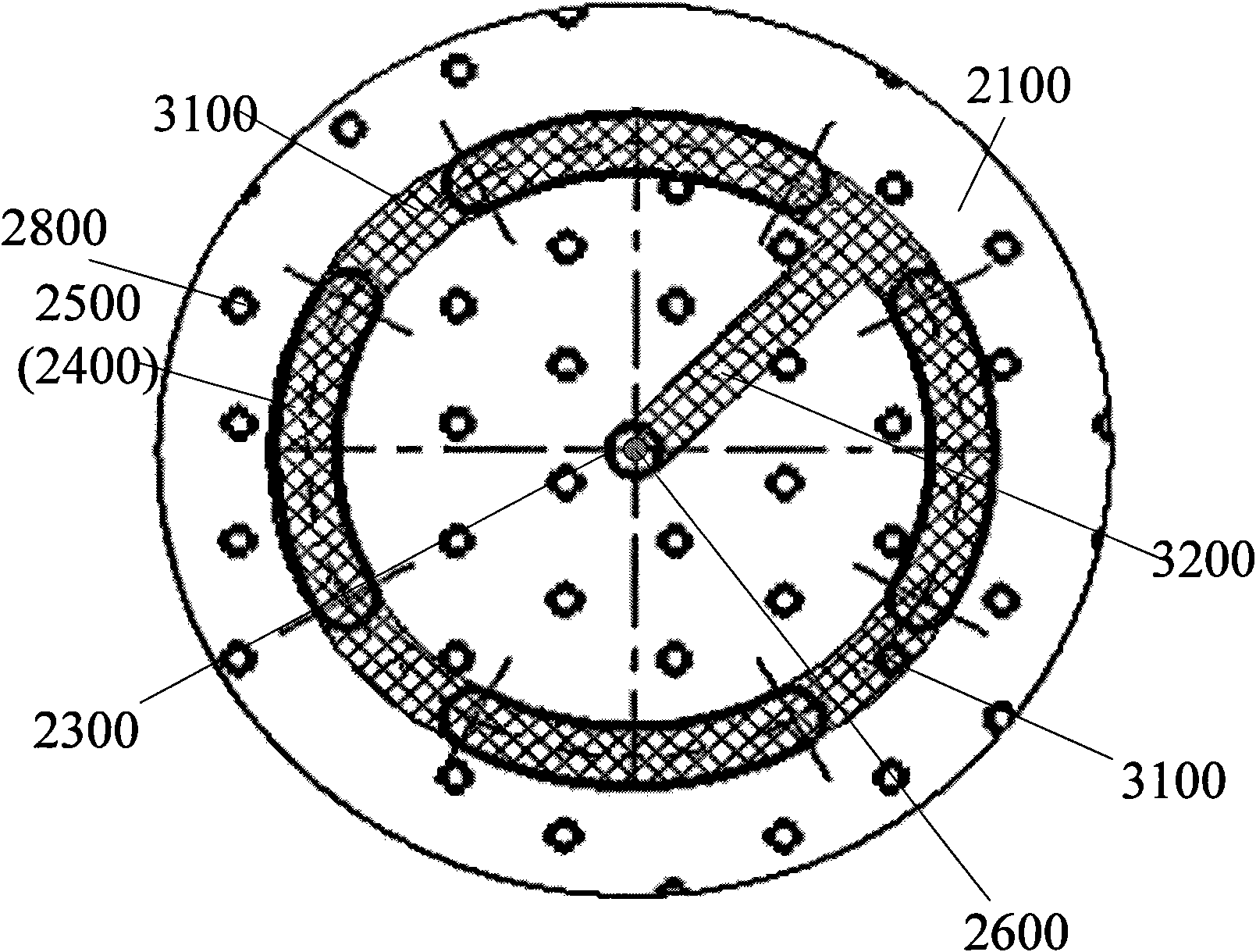
The invention provides an electrostatic chuck. The electrostatic chuck comprises a chuck body, an electrode layer, a conducting piece, a plurality of convex parts, a boss and a conducting layer, wherein the chuck body is provided with an air inlet hole and an installing hole; the electrode layer is arranged in the chuck body; the conducting piece is fixedly arranged in the installing hole; the convex parts are arranged on the upper surface of the chuck body, and a gas channel is formed on the upper surface of the chuck body and is communicated with the air inlet hole; the boss is arranged on the upper surface of the chuck body; the conducting layer is arranged on the upper surface of the boss and is electrically connected with the conducting piece; and the upper surface of the conducting layer is level to the upper surfaces of the convex parts. According to the embodiment of the invention, by the boss and the conducting layer arranged on the upper surface of the chuck body, the conducting piece can be fully contacted with a chip; and since the boss and the conducting layer provide a larger contact surface, the diameter of the conducting piece can be reduced, so that the generation of enough adsorptive force for the chip by the electrostatic chuck can be ensured.

Description

technical field [0001] The invention relates to the technical field of microelectronics, in particular to an electrostatic chuck and a plasma device with the electrostatic chuck. Background technique [0002] In the integrated circuit manufacturing process, especially in plasma etching (ETCH), physical vapor deposition (PVD), chemical vapor deposition (CVD) and other processes, in order to fix, support and transfer the wafer and realize temperature control, avoid in the process If there is movement or misalignment in the wafer, a chuck is often used to hold the wafer. Due to the irreparable damage to the wafer caused by mechanical reasons such as pressure and collision, the electrostatic chuck has gradually replaced the traditional mechanical chuck. [0003] A typical electrostatic chuck usually consists of two parts, an insulating layer and an aluminum base. The insulating layer is currently manufactured by processing ceramic materials, or in the form of ceramic spraying,...

Claims


Application Information

Patent Timeline
Patent Type & Authority Applications(China)
IPC IPC(8): H01L21/683H01J37/32
Inventor 武学伟赵梦欣丁培军
Owner BEIJING NAURA MICROELECTRONICS EQUIP CO LTD
Learn More