Semiconductor device and manufacture method thereof

A manufacturing method and semiconductor technology, applied in semiconductor/solid-state device manufacturing, semiconductor devices, semiconductor/solid-state device components, etc., can solve problems such as large RC delay, source-drain doping concentration is no longer practical, and device performance is degraded. Achieve the effect of reducing RC delay, eliminating parasitic capacitance, and improving device switching performance

Active Publication Date: 2012-06-06
INST OF MICROELECTRONICS CHINESE ACAD OF SCI
View PDF5 Cites 3 Cited by
  • Summary
  • Abstract
  • Description
  • Claims
  • Application Information

AI Technical Summary

Problems solved by technology

However, due to the solid solubility limit and the shallow doping structure required to suppress the short-channel effect, increasing the source-drain doping concentration becomes impractical
[0009] At the same time, although the capacitance between the gate and source-drain can be greatly reduced or even eliminated by reducing the width of the isolation spacer, the current Salicide process requires the isolation spacer as a mask to form metal silicide, and the isolation spacer must have A certain thickness, so the reduction of parasitic capacitance is limited
[0010] Therefore, the traditional MOSFET has a large parasitic resistance and capacitance due to the spacing between the isolation sidewall and the contact hole, resulting in a huge RC delay and a significant drop in device performance

Method used


Image

  • Semiconductor device and manufacture method thereof
  • Semiconductor device and manufacture method thereof
  • Semiconductor device and manufacture method thereof

Examples


Embodiment Construction

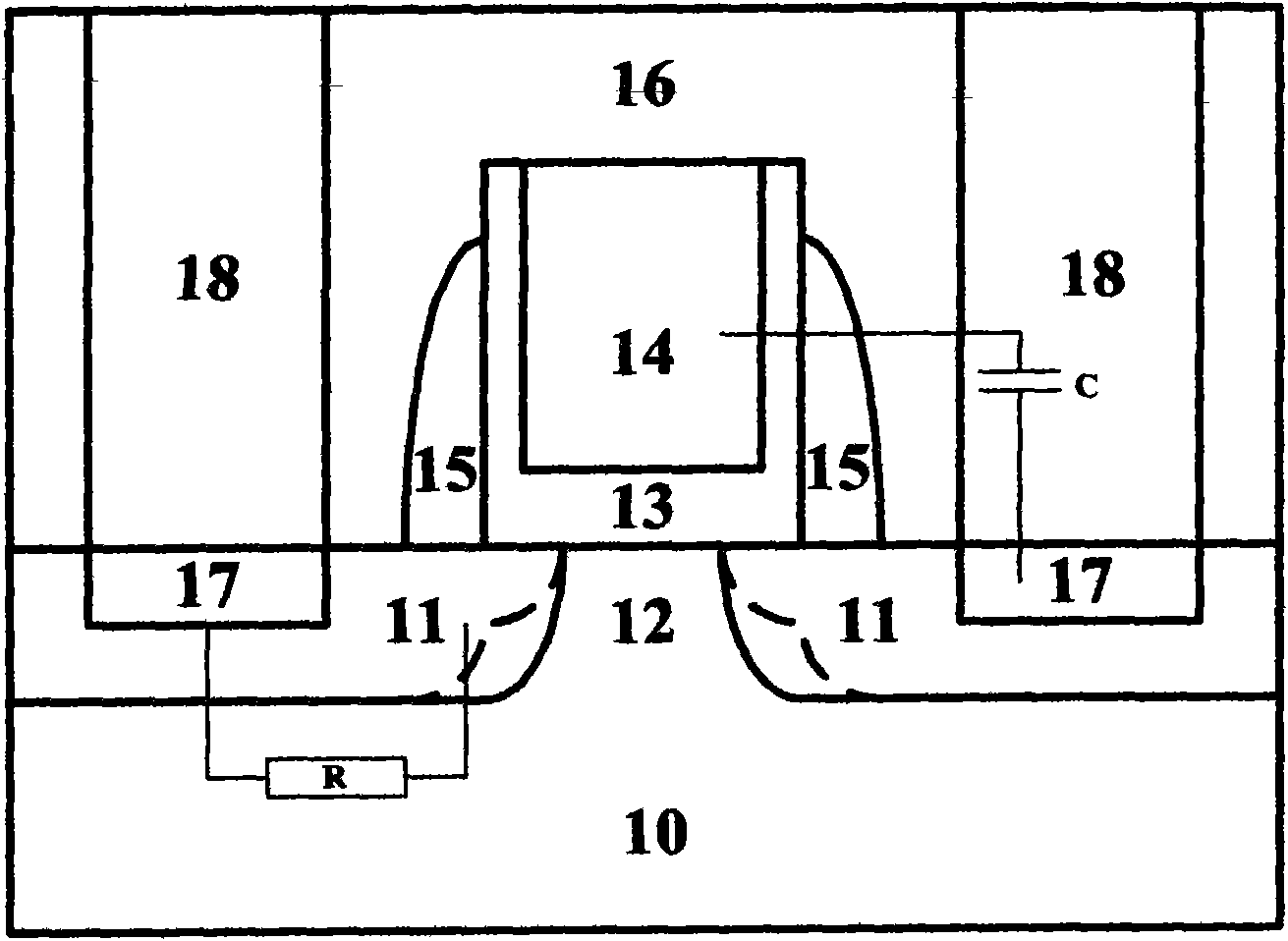
[0035] The features and technical effects of the technical solution of the present invention will be described in detail below with reference to the accompanying drawings and in conjunction with exemplary embodiments, and a novel semiconductor device structure and a manufacturing method thereof that can effectively reduce RC delay are disclosed. It should be pointed out that similar reference signs indicate similar structures, and the terms "first", "second", "upper", "lower", etc. used in this application can be used to modify various device structures. Unless otherwise specified, these modifications do not imply the spatial, order, or hierarchical relationship of the modified device structure.

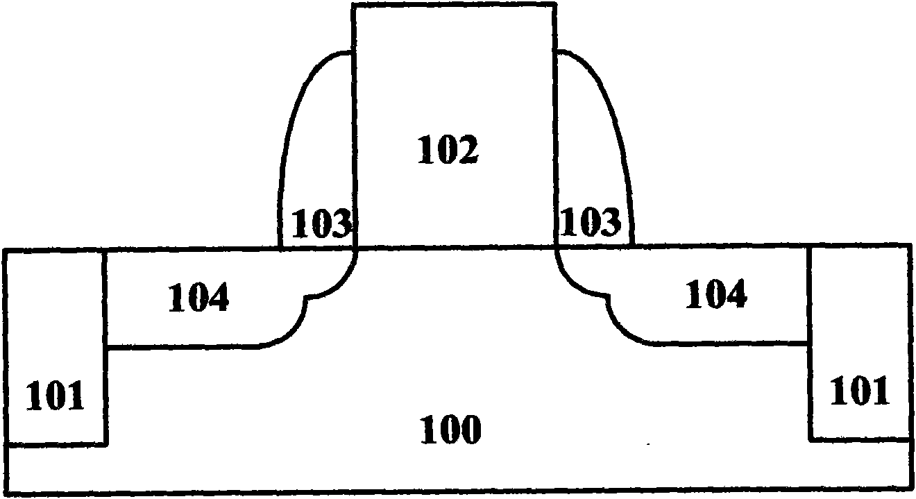
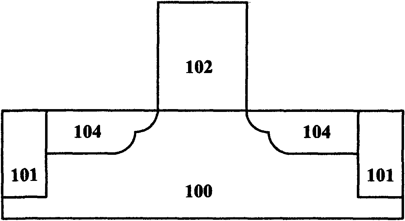
[0036] First, a commonly used process is used to form a lightly doped source-drain (LDD) structure. Such as figure 2 Shown is a schematic cross-sectional view of the LDD structure. On the Si substrate 100 with shallow trench isolation (STI) 101, a thick oxide such as silicon oxide, es...


PUM


Abstract

The invention discloses a novel MOSFET (Metal-Oxide -Semiconductor Field Effect Transistor) device and a realization method thereof. The MOSFET device comprises a substrate, a grid electrode stacking structure, source and drain regions and epitaxially-grown metal silicide, wherein the grid electrode stacking structure is positioned on a channel; the traditional isolated side walls on the left and the right of the grid electrode stacking structure are eliminated; the source and drain regions are positioned in the substrate region on two grid electrode stacking sides; and the epitaxially-grown metal silicide is positioned on the source and drain regions. The MOSFET device is characterized in that the epitaxially-grown metal silicide directly contacts with the channel subjected to grid electrode stacking control so as to eliminate a high-resistance zone below the isolated side walls; meanwhile, the epitaxially-grown metal silicide can bear secondary high-temperature annealing carried out for improving the performance of a k grid dielectric material so as to further improve device performance. According to the MOSFET disclosed by the invention, the capacitance of parasitic resistance is greatly reduced so as to reduce RC (Resistance-Capacitance) delay, and therefore, the switching performance of the MOSFET device is greatly improved.

Description

Technical field [0001] The invention relates to a semiconductor device and a manufacturing method thereof, in particular to a novel semiconductor device structure and a manufacturing method thereof that can effectively reduce RC delay. Background technique [0002] The continuous increase of IC integration requires continuous scaling down of the device size, but the working voltage of the electrical appliance sometimes remains unchanged, which makes the actual electric field strength in the MOS device continuously increase. The high electric field brings a series of reliability problems, which degrades the performance of the device. [0003] For example, when the gate oxide layer is continuously thinning, the electric field strength is too large to cause breakdown of the oxide layer, resulting in leakage of the gate oxide layer, and destroying the insulation of the gate dielectric layer. In order to reduce gate leakage, use high-k dielectric materials to replace SiO 2 As the gate ...

Claims


Application Information

Patent Timeline
Patent Type & Authority Applications(China)
IPC IPC(8): H01L29/78H01L29/417H01L23/52H01L21/336H01L21/768
CPCH01L29/66545H01L29/7833H01L29/78H01L23/52H01L29/417H01L21/768H01L29/66606H01L2924/0002H01L2924/00
Inventor 罗军赵超
Owner INST OF MICROELECTRONICS CHINESE ACAD OF SCI
Why Eureka
Try Eureka