Transistor and forming method thereof

A technology of transistors and semiconductors, applied in the manufacture of transistors, semiconductor devices, semiconductor/solid-state devices, etc., can solve problems such as poor performance of transistors, and achieve the effects of eliminating signal delay, improving performance, and improving mobility

Active Publication Date: 2014-04-09
SEMICON MFG INT (SHANGHAI) CORP
View PDF6 Cites 4 Cited by
  • Summary
  • Abstract
  • Description
  • Claims
  • Application Information

AI Technical Summary

Problems solved by technology

[0010] The problem solved by the present invention is that the performance of transistors with stress liner layers formed by using embedded silicon germanium technology in the prior art is not good

Method used


Image

  • Transistor and forming method thereof
  • Transistor and forming method thereof
  • Transistor and forming method thereof

Examples


Embodiment Construction

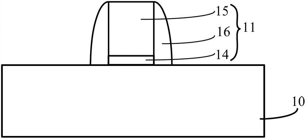
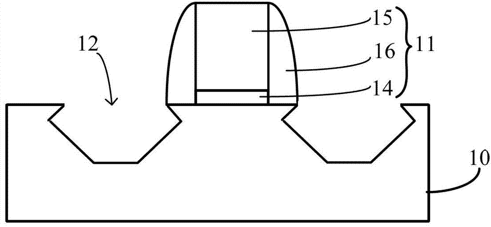
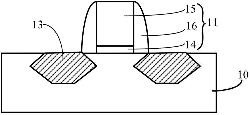
[0050] The inventor analyzed the problems existing in the prior art and found that as the integration of semiconductor devices becomes higher and higher, the distance between the gates gradually decreases, further making the distance between the silicon germanium layer and the gate The smaller and smaller, the parasitic capacitance is generated between the gate and the silicon germanium layer. Moreover, according to the description in the background art, after the stress liner layer is formed in the semiconductor substrate, an additional stress liner layer extending to the outside of the semiconductor substrate is formed on the stress liner layer, so that the gate and the additional stress The relative area between the liner layers increases, resulting in a larger parasitic capacitance between the gate and the entire stressed liner layer including the additional stressed liner layer. Although the additional stress of the liner layer increases the carrier mobility of the transi...


PUM


Abstract

The invention relates to a transistor and a forming method thereof. The forming method comprises the following steps that: a semiconductor substrate is provided; gate structures are formed at the semiconductor substrate, wherein the gate structures include gate dielectric layers formed at the semiconductor substrate and gate electrodes arranged at the gate dielectric layers and first side walls are formed at the semiconductor substrate around the gate structures; a sigma-shaped groove is formed in the semiconductor substrate at the two sides of the gate structures; a first stress liner layer is formed in the sigma-shaped groove, wherein the surface of the first stress liner layer is flush with the surface of the substrate; second side walls are formed around the first side walls; a second stress liner layer is formed on the first stress liner layer, wherein the thickness of the second stress liner layer is less than or equal to the height of the second side wall. Because of the second side walls, the distance between the second stress liner layer and the gate structures to be enlarged; the parasitic capacitance between the second stress liner layer and the gate structures is reduced or even eliminated; and the semiconductor device performance is improved.

Description

technical field [0001] The invention relates to the technical field of semiconductors, in particular to a method for forming a transistor and the transistor. Background technique [0002] In the existing manufacturing process of semiconductor devices, since stress can change the energy gap and carrier mobility of silicon materials, it has become an increasingly common means to improve the performance of MOS transistors through stress. Specifically, by properly controlling the stress, the mobility of carriers (electrons in NMOS transistors and holes in PMOS transistors) can be increased, thereby increasing the driving current, thereby greatly improving the performance of MOS transistors. For PMOS transistors, embedded silicon germanium technology (Embedded SiGe Technology) can be used to generate compressive stress in the channel region of the transistor, thereby improving carrier mobility. The so-called embedded silicon germanium technology refers to embedding silicon germa...

Claims


Application Information

Patent Timeline
Patent Type & Authority Applications(China)
IPC IPC(8): H01L21/336H01L29/78
CPCH01L29/6656H01L29/66568H01L29/66636H01L29/7848
Inventor 韩秋华隋运奇
Owner SEMICON MFG INT (SHANGHAI) CORP
Why Eureka
Try Eureka