Inductor

Active Publication Date: 2011-08-18
FUJI ELECTRIC CO LTD
View PDF4 Cites 4 Cited by
  • Summary
  • Abstract
  • Description
  • Claims
  • Application Information

AI Technical Summary

Benefits of technology

[0037]According to the invention, total parasitic capacitance can be reduced in the inductor. It is therefore possible to reduce the loss in a switching device when the inductor is applied to a conversion

Problems solved by technology

First, when a high-frequency current flows in a conducting wire, the current generally flows only near the surface of the conducting wire due to skin effect so as to increase loss.
In addition, parasitic capacitance generated between wires not adjacent to each other takes a small value due to a long distance between the wires not adjacent to each other.
Further, when adjacent conductors have the same potential, energy cannot be stored in parasitic capacitance generated between the adjacent conductors.
When an inductor having such a large parasitic capacitance is used in a conversion circuit or the like, there arises the problem that the current for charging/discharging the parasitic capacitance increases and hence loss or high-frequency noise increases.
Thus, the appara

Method used


Image

  • Inductor
  • Inductor
  • Inductor

Examples


Example

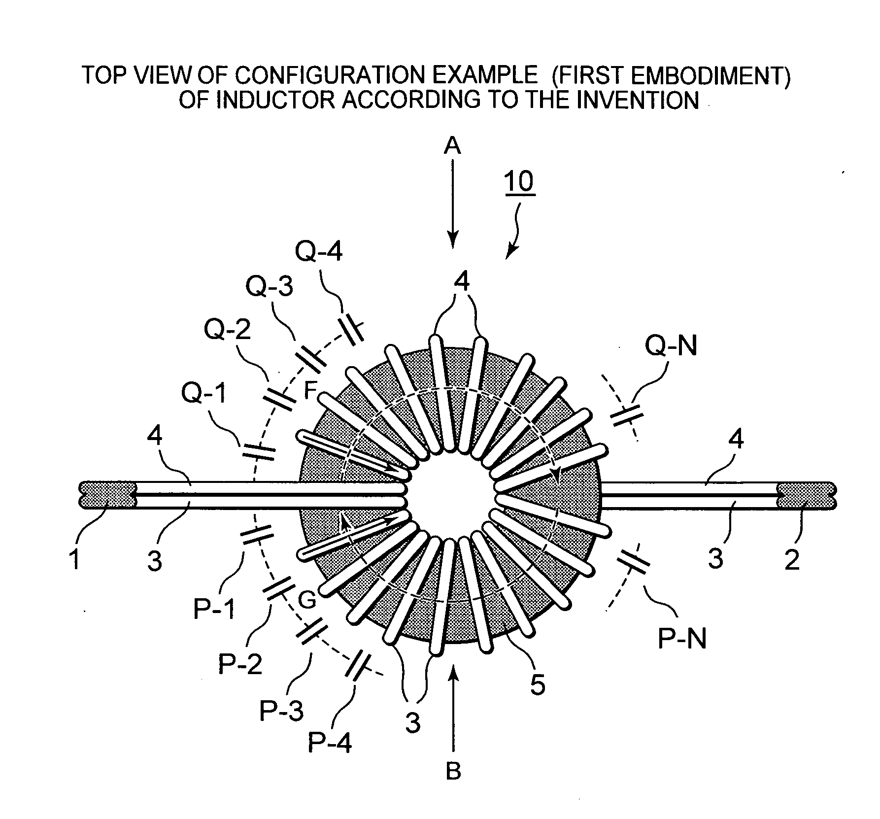
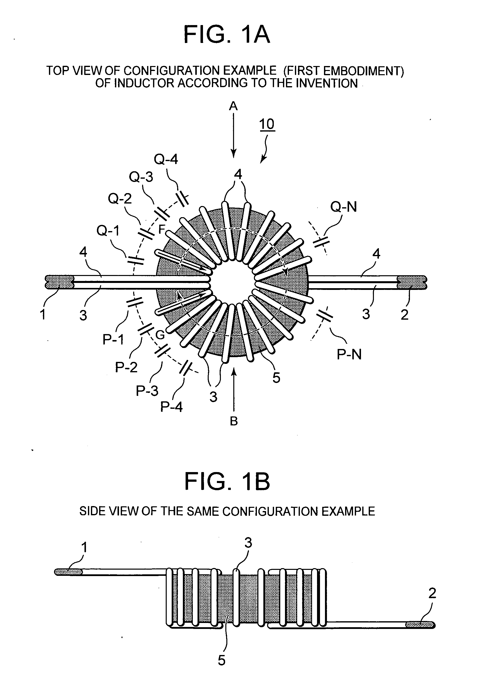
[0045]FIGS. 1A and 1B are diagrams showing a configuration example (first embodiment) of an inductor according to the invention. FIG. 1A is a top view and FIG. 1B is a side view.

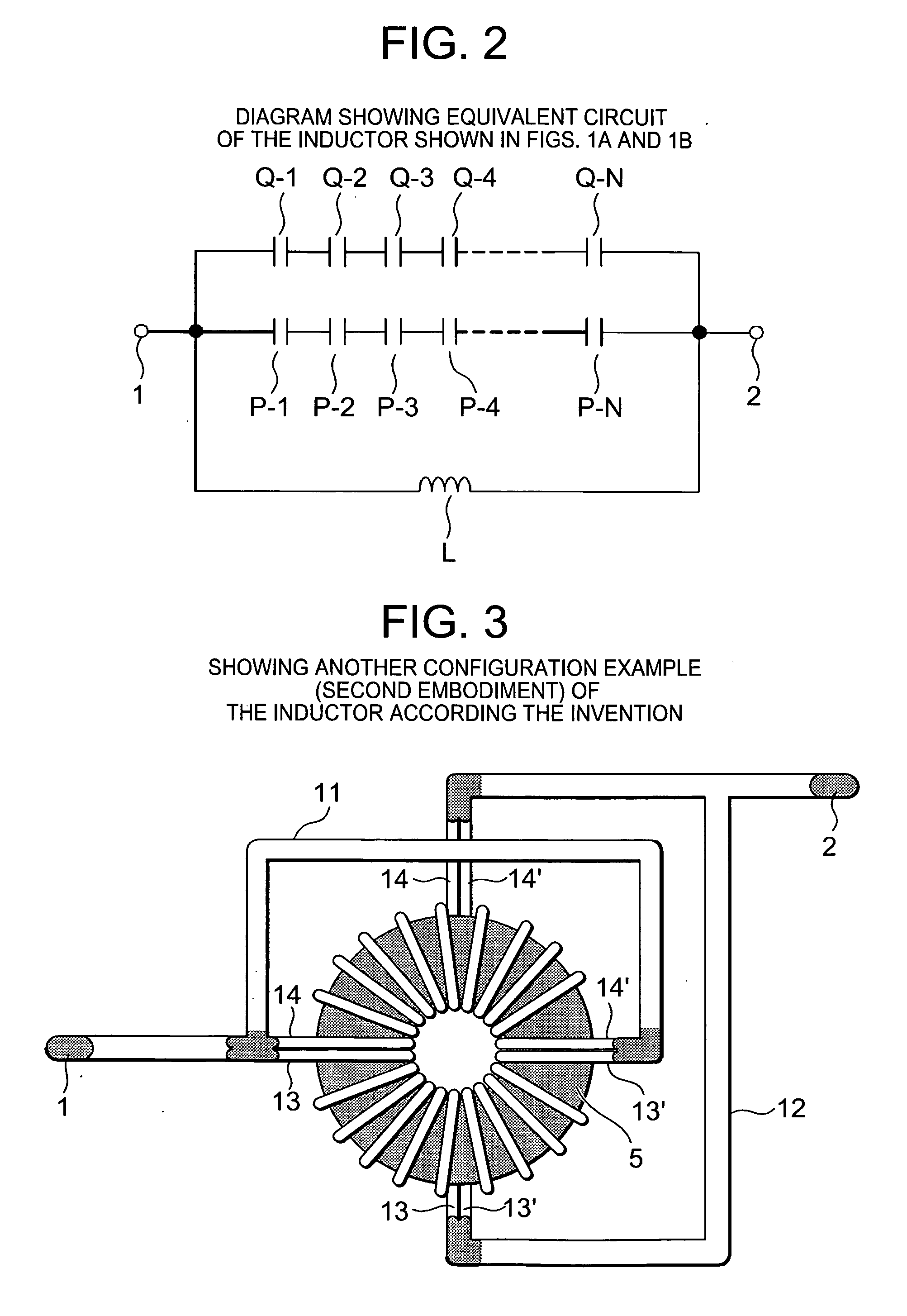
[0046]FIG. 2 is a diagram showing an equivalent circuit of the inductor shown in FIGS. 1A and 1B.

[0047]Also in this embodiment, a configuration in which a plurality of conducting wires are wound around a magnetic substance 5 is used fundamentally in the same manner as in the background-art inductor shown in FIGS. 4A and 4B. In an inductor 10 shown in FIGS. 1A and 1B, two conducting wires 3 and 4 are used to form windings. The opposite ends of each conducting wire 3, 4 are connected to shared terminals (leader lines 1 and 2), and the conducting wires 3 and 4 are connected in parallel between the leader line (terminal) 1 and the leader line (terminal) 2.

[0048]The reason why a plurality of conducting wires (two conducting wires 3 and 4 in this embodiment) are used is to increase the surface area and increase th...

Example

[0092]FIG. 3 is a diagram showing another configuration example (second embodiment) of the inductor according to the invention. Only a top view is shown in FIG. 3. Therefore, a side view is absent from FIG. 3. FIG. 3 may be regarded as an example where four conducting wires are used as windings.

[0093]Four conducting wires, i.e. conducting wires 13, 13′, 14 and 14′ are used as illustrated in FIG. 3. In FIG. 3, the reference numeral is attached to the opposite ends of each of the four conducting wires. To take the conducting wire 13 as an example, the reference numeral “13” is attached to one end and the other end of the conducting wire 13. In this manner, the portion on which each conducting wire is wound in the magnetic substance 5 will be understood with reference to FIG. 3.

[0094]That is, according to this embodiment, four conducting wires are used. Accordingly, the magnetic substance 5 is divided into four areas. The four conducting wires are wound around the four areas respective...


PUM


Abstract

Two conducting wires are used in one embodiment of an inductor. Opposite ends of each of the conducting wires are connected to leader lines (terminals) shared by the conducting wires. Each of the conducting wires is wound to make half a round of an annular or ring-like magnetic substance. One of the conducting wires is wound around a lower half area of the magnetic substance to form one winding while the other conducting wire is wound around an upper half area of the magnetic substance to form another winding. In this manner, the distance between the leader lines can be increased to eliminate parasitic capacitance between the leader lines. The magnetic fluxes generated by current flowing in the two windings are in the same direction. Thus, it is possible to provide an inductor whose total parasitic capacitance is reduced. In other embodiments, additional conducting wires are used.

Description

CROSS-REFERENCE TO RELATED APPLICATION[0001]This application claims the benefit of foreign priority of Japanese application 2010-029204, filed Feb. 12, 2010, the disclosure of which is incorporated herein by reference.BACKGROUND OF THE INVENTION[0002]1. Field of the Invention[0003]The present invention relates to an inductor.[0004]2. Description of the Background Art[0005]In the background art, there has been known an electronic component, that is, a so-called inductor, in which conducting wires are wound around a magnetic substance to obtain a desired inductance value or conducting wires are wound around an air core (such as a nonmagnetic bobbin, or nothing to serve as a core) to obtain a desired inductance value.[0006]FIGS. 4A and 4B show a configuration example of a background-art inductor. FIG. 4A is a top view, and FIG. 4B is a side view.[0007]A background-art inductor 50 has a configuration, for example, in which windings are formed by winding conducting wires around a magneti...

Claims


Application Information

Patent Timeline
IPC IPC(8): H01F27/28
CPCH01F17/06
Inventor MINO, KAZUAKI
Owner FUJI ELECTRIC CO LTD
Why Eureka
Try Eureka