Input vector monitoring concurrency built-in self-test circuit based on comparator and response analyzer
A built-in self-test and response analysis technology, which is applied in the field of SOC test equipment, can solve the problems of large input pin test delay, high hardware cost, and unmonitorable circuits, so as to reduce hardware cost and concurrent test delay. when the effect
- Summary
- Abstract
- Description
- Claims
- Application Information
AI Technical Summary
Problems solved by technology
Method used
Image

Examples
specific Embodiment approach 1
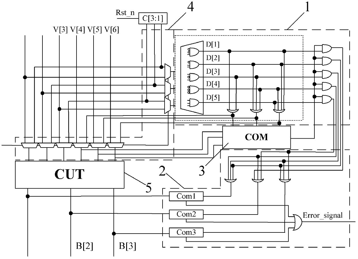
[0013] Specific implementation mode one: combine figure 1 Describe this embodiment, the input vector monitoring and built-in self-test circuit based on the comparator response analyzer of this embodiment includes a test set generator 1, an output response analyzer 2, a comparator 3 and a multiplexer 4 ;
[0014] The integrated circuit 5 under test has an n-bit input terminal, the input signal of the input terminal is the original input signal output by the upper stage circuit, and the original input signal output by the upper stage circuit is a 0 or 1 signal, and the n-bit upper stage In the original input signal output by the circuit, t bits are selected as the address signal output by the upper circuit, and the remaining n-t bits are used as non-address signals output by the upper circuit, wherein, log 2 T ≤ t ≤ n ,
[0015] The number of two-to-one multiplexers 4 is...
specific Embodiment approach 2
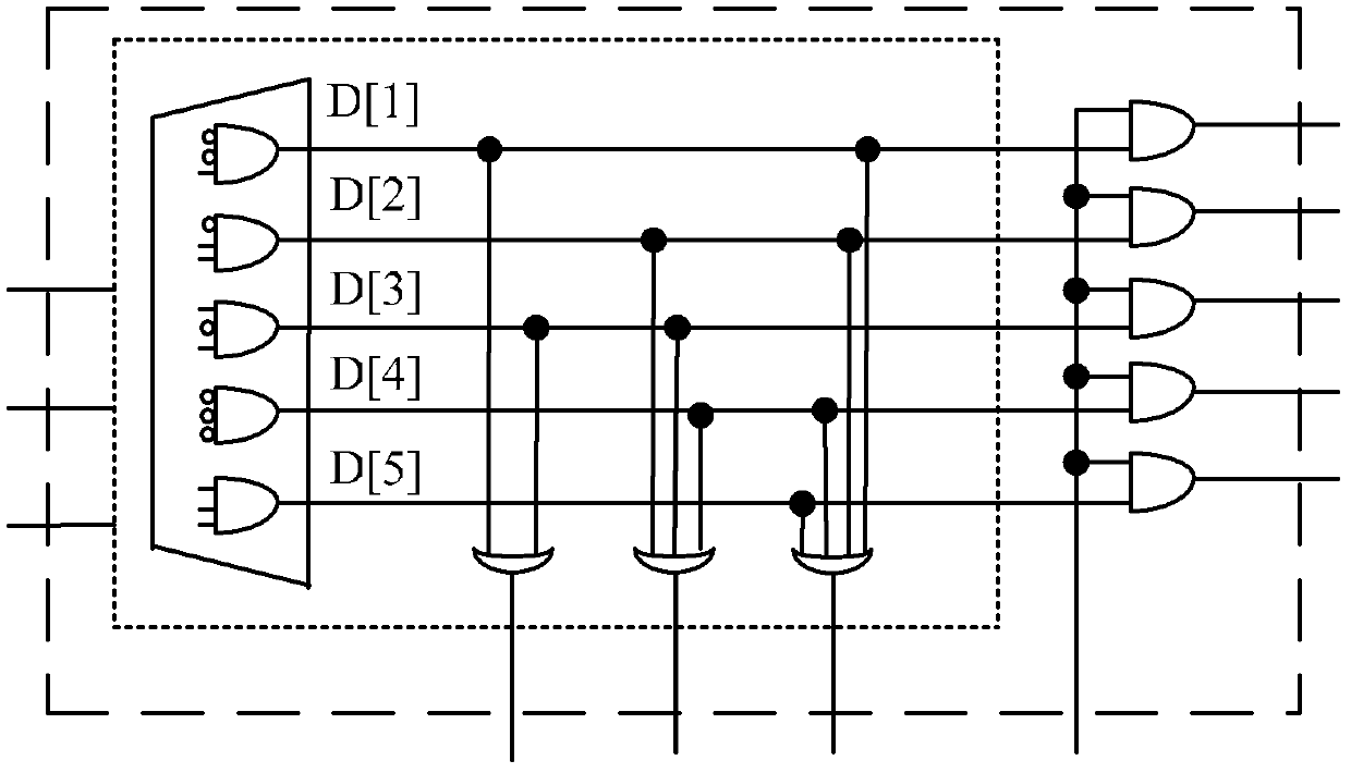
[0023] Specific implementation mode two: combination figure 2 Describe this embodiment, the difference between this embodiment and the specific embodiment is that the test set generator 1 includes T test vectors, T row output AND gates and n-t column output OR gates;
[0024] The t input terminals of the test set generator 1 receive the t-bit address signal output by the upper-level circuit, and the t-bit address signal output by the upper-level circuit is combined into a plurality of different input signals, and each input signal corresponds to a test vector , and send the corresponding input signal to the input of the test vector generator,
[0025] The number of the test vectors is T, and the number of bits of each test vector is n, then the test set in the test set generator 1 forms a matrix of T×n;
[0026]
[0027] The t columns in the n columns in the matrix are selected as address bits, and each row in the test set is formed into a T×n matrix as a set, if the subs...
specific Embodiment approach 3
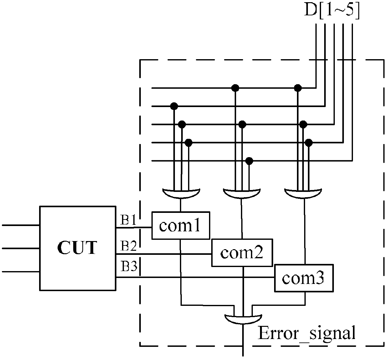
[0038] Specific implementation mode three: combination image 3 Describe this embodiment, the difference between this embodiment and the specific embodiment 1 or 2 is that the output response analyzer 2 includes m OR gates and m response analysis comparators, and the input bus of the output response analyzer 2 is the response analyzer 2 The signal input terminal, the signal output by the input bus corresponds to an OR gate, when the signal output by the input bus is at a high level, the input terminal of the OR gate receives a logic value 1, and the output terminal of the OR gate outputs a logic value 1, or The output end of the gate is connected to the test signal input end of the response analysis comparator, the actual signal input end of the response analysis comparator is the actual signal input end of the response analyzer 2, and the actual signal input end of the response analysis comparator is connected to the integrated circuit 5 under test The output terminals of the...
PUM
 Abstract
Description
Claims
Application Information
 - R&D
- Intellectual Property
- Life Sciences
- Materials
- Tech Scout
- Unparalleled Data Quality
- Higher Quality Content
- 60% Fewer Hallucinations
Browse by: Latest US Patents, China's latest patents, Technical Efficacy Thesaurus, Application Domain, Technology Topic, Popular Technical Reports.
© 2025 PatSnap. All rights reserved.Legal|Privacy policy|Modern Slavery Act Transparency Statement|Sitemap|About US| Contact US: help@patsnap.com