

Method for manufacturing resistance-type touch screen and resistance-type touch screen
A touch screen, resistive technology, applied in the direction of electrical digital data processing, input/output process of data processing, instruments, etc., can solve the problems of difficult process, etc., achieve the effect of thin thickness, reduce production cost, and save man-hours
- Summary
- Abstract
- Description
- Claims
- Application Information
AI Technical Summary
Problems solved by technology
Method used
Image

Examples
Embodiment Construction
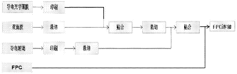
[0041] Refer to attached picture. The method for preparing a resistive touch screen provided by the present invention includes a preparation step of a conductive optical film and a preparation step of a conductive glass;
[0042] The preparation steps of the conductive optical film include:
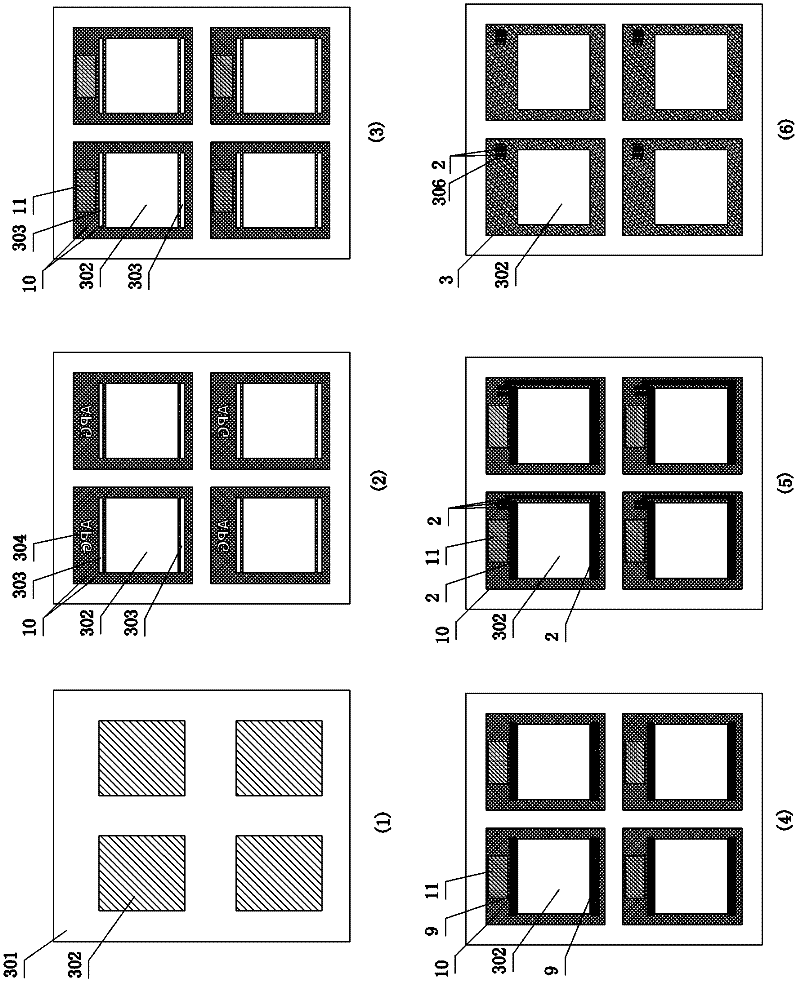
[0043] 1. see figure 2 Part (1) of the raw material conductive optical film 301 is partially etched to obtain the required conductive touch operation area 302; the etching methods include laser etching and acid etching. From figure 2 It can be seen in part (1) that the raw conductive optical film 301 accommodates four electro-optical film units adapted to the touch screen (according to the actual situation, other numbers can be selected for the typesetting capacity). The following steps are described in terms of The electro-optic film with a touch screen unit and the preparation process of the conductive glass are described.
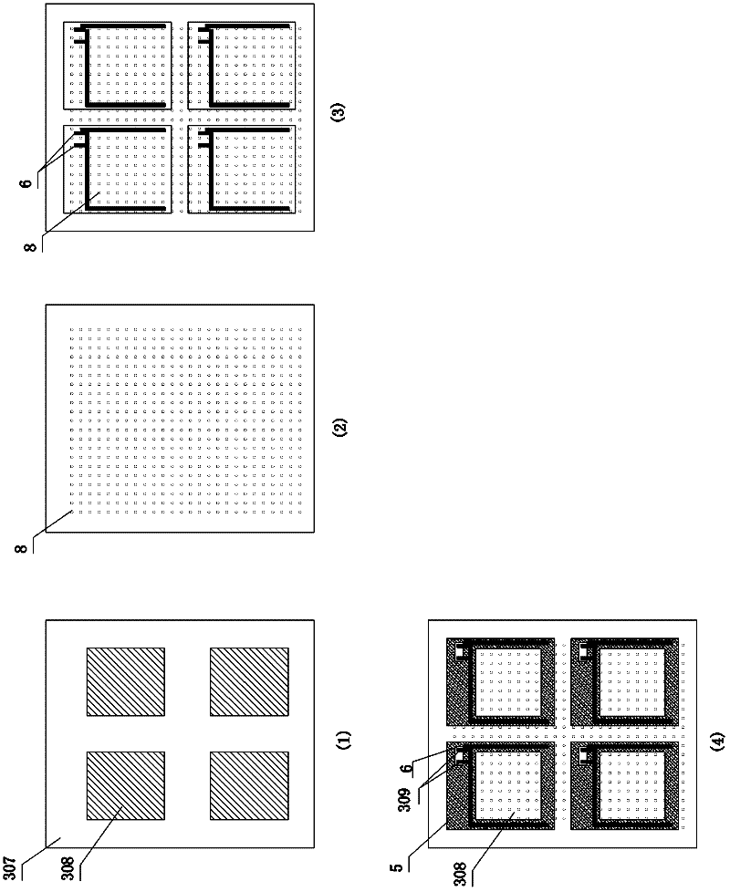
[0044] 2. see figure 2 In parts (2) and (3), the first...
PUM
 Abstract
Description
Claims
Application Information