Electromagnetic band gap structure, electromagnetic band gap high-impedance substrate and planar travelling wave tube

An electromagnetic bandgap structure and electromagnetic bandgap technology, applied in the field of physical electronics, can solve the problems of increasing the lateral size of the substrate, increasing the substrate area, unfavorable for manufacturing miniaturized equipment, etc., and achieving increased working bandwidth, simple process, and optimization. Effects of Dispersion Characteristics and Coupling Impedance Characteristics

Inactive Publication Date: 2012-06-27
SOUTHEAST UNIV
View PDF4 Cites 6 Cited by
  • Summary
  • Abstract
  • Description
  • Claims
  • Application Information

AI Technical Summary

Problems solved by technology

But existing EBG structures such as figure 1 The EBG structure shown ( figure 2 is the bandgap diagram of the structure), it must be arranged periodically in both dimensions to achieve the effect of forming a bandgap, which will increase the lateral size of the substrate and increase the substrate area, which is not conducive to the manufacture of miniaturized equipment

Method used


Image

  • Electromagnetic band gap structure, electromagnetic band gap high-impedance substrate and planar travelling wave tube
  • Electromagnetic band gap structure, electromagnetic band gap high-impedance substrate and planar travelling wave tube
  • Electromagnetic band gap structure, electromagnetic band gap high-impedance substrate and planar travelling wave tube

Examples


Embodiment Construction

[0025] The technical scheme of the present invention is described in detail below in conjunction with accompanying drawing:

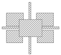
[0026] In the electromagnetic bandgap structure of the present invention, there is no specific requirement on the shapes of the two groups of closed metal curves, as long as the shapes of the two groups are different. The electromagnetic bandgap structure formed by two sets of metal closed curves, which are square and circular, respectively, will be described below as an example. This structure is simpler to manufacture.

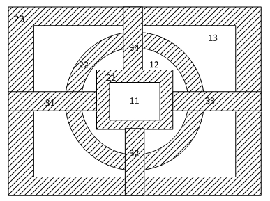
[0027] Such as image 3 As shown, the electromagnetic bandgap structure in this embodiment includes two groups of metal closed curves of different shapes, wherein one group is square 21, 23, 21 and 23 have the same shape and different size; the other group is circular 22 Two groups of metal closed curves are overlapped and surrounded sequentially from inside to outside; metal closed curves 21, 22, 23 are connected to each other by me...


PUM


Abstract

The invention discloses an electromagnetic band gap structure. The electromagnetic band gap structure comprises two groups of metal closed curves with different shapes, wherein all metal closed curves in each group have the same shape and different sizes; the two groups of metal closed curves sequentially surround each other from inside to outside in an overlapped mode; and the distance between the two adjacent metal closed curves in the same group is equal to the distance between the innermost metal closed curve in the group and a central point of an area which is surrounded by the innermost metal closed curve. The invention also discloses an electromagnetic band gap high-impedance substrate and a planar travelling wave tube with the electromagnetic band gap high-impedance substrate. The invention has the advantages that: stop-band bandwidth is large, stop-band attenuation is high, and the edge of a transmission curve is straight; a requirement of a slow wave structure for the surface wave suppression of a microwave frequency band can be well met, the coupling impedance of the slow wave structure is effectively improved, and the working bandwidth of the slow wave structure is increased; and a manufacturing process is simple, the transverse size of the conventional planar structure cannot be increased, and a magnetic field can be designed.

Description

technical field [0001] The invention relates to an electromagnetic bandgap structure, which belongs to the technical field of physical electronics. Background technique [0002] The slow wave structure is mainly used in traveling wave amplifiers, particle accelerators, and devices that interact between electromagnetic waves and waves of lower speed (such as sound waves, magnetostatic waves, etc.), and its role is to make the interaction over a longer distance and a longer time Ongoing. In this system, the phase velocity of electromagnetic waves is lower than the speed of light in space, so that the energy of moving charged electron particles or low-speed waves can be effectively converted into the energy of electromagnetic waves. [0003] Miniaturization and planar traveling wave tubes are the main ways to reduce the manufacturing cost of traveling wave tubes, reduce the volume and break through the upper limit of frequency. Pioneering and innovating in the key components ...

Claims


Application Information

Patent Timeline
IPC IPC(8): H01J25/34H01J23/36
Inventor 柏宁丰孙小菡
Owner SOUTHEAST UNIV
Why Eureka
Try Eureka