Method for forming solar dry textured black silicon by plasma excitation

A technology of solar cells and silicon wafers, applied in the manufacture of circuits, electrical components, and final products, can solve problems such as waste of process time, high cost, and difficulty in uniformity control, and achieve increased production capacity, increased utilization, and ion bombardment The effect of little damage

Active Publication Date: 2014-01-08
江苏杰太光电技术有限公司
View PDF14 Cites 3 Cited by
  • Summary
  • Abstract
  • Description
  • Claims
  • Application Information

AI Technical Summary

Problems solved by technology

[0006] The current RIE dry etching is completed under static conditions, that is to say, the carrier plate is placed under the ion source and does not move until the etching is completed, then it is taken out, and then another carrier plate (silicon wafer) is placed. In this way, the carrier board transfer process wastes process time
Therefore, in order to achieve high productivity (the ability to process silicon wafers per unit time), the carrier board must be made very large, and a large number of silicon wafers are placed. The cost of such large-scale equipment is very high, and the uniformity is difficult to control

Method used


Image

  • Method for forming solar dry textured black silicon by plasma excitation
  • Method for forming solar dry textured black silicon by plasma excitation

Examples


Embodiment Construction

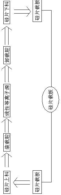
[0025] Such as figure 1 with figure 2 As shown, the method is realized by an automatic conveying device, including silicon wafer carrier, silicon wafer loading and silicon wafer unloading. The specific process steps are as follows:

[0026] 1. The automatic transfer device drives the silicon wafer carrier 3, and places the silicon wafer 4 to be etched on the silicon wafer carrier through silicon wafer loading;

[0027] 2. The silicon wafer carrier plate 3 carrying the silicon wafer 4 passes through a group of linear plasma sources placed in parallel under the drive of the automatic transport device, and the silicon wafer carrier plate 3 loaded with the silicon wafer 4 is driven by the automatic transport device in a vacuum Pass through the linear plasma source at a speed of 30-3000mm / min;

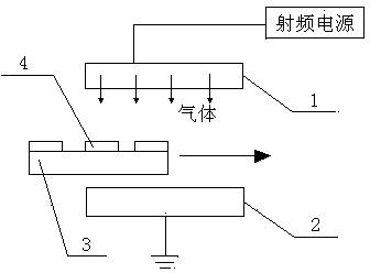
[0028] The linear plasma source is composed of a pair of parallel plates, the first plate 1 of the parallel plates is connected to the radio frequency power supply, the second plate 2 is...


PUM

PropertyMeasurementUnit
widthaaaaaaaaaa
lengthaaaaaaaaaa
diameteraaaaaaaaaa

Abstract

The invention relates to a method for forming black silicon, in particular to a method for forming solar dry textured black silicon by plasma excitation. The method comprises the following steps that: 1, an automatic transmission device drives a silicon chip support plate, and a silicon chip which is needed to be etched is placed on the silicon chip support plate by a silicon chip loading device; 2, the silicon chip support plate loaded with the silicon chip passes through a linear plasma source which consists of parallelly-arranged plates at certain speed in vacuum under the drive of the automatic transmission device; 3, gas obtained after etching is extracted by a vacuum pump and a guide pipe thereof; and 4, the silicon chip on the silicon chip support plate is unloaded by a silicon chip unloading device, and a finished black silicon product is obtained. The method has the advantages that: plasma has high density and low surface damage to the surface of the silicon, so that the obtained black silicon battery plate has high conversion efficiency; meanwhile, etching speed is high, so that yield is increased; and in addition, the support plate is placed on a grounding electrode, so that the plasma source is more stable.

Description

technical field [0001] The invention relates to a method for forming black silicon for solar cell production, in particular to a method for forming solar dry texturing black silicon by plasma excitation. Background technique [0002] The manufacture of solar cells has developed rapidly in recent years, and there are already 100GW installed capacity of power stations around the world using crystalline silicon solar power. In order to make solar power generation more commercially advantageous, the industry is constantly seeking technological innovations to achieve higher photoelectric conversion efficiency, lower production costs, and minimal environmental impact. [0003] Dry texturing is a technology that has only recently begun to be industrialized. It uses chemical etching in vacuum to roughen the surface of the original smooth silicon wafer at the nanometer level, reducing the reflectivity of incident light on the silicon surface from 30% to Below 10%, compared with trad...

Claims


Application Information

Patent Timeline
Patent Type & Authority Patents(China)
IPC IPC(8): C23F4/00H01L31/18
CPCY02P70/50
Inventor 上官泉元刘金浩解观超朱广东
Owner 江苏杰太光电技术有限公司
Why Eureka
Try Eureka