Nanofluidic chip, processing method based on atomic force microscopy (AFM), and application

A nanofluidic and chip technology, applied in the direction of nanotechnology, nanotechnology, nanotechnology for sensing, etc., can solve the problems of easily damaged samples, expensive, easy to leave residues, etc., to achieve accurate cost, fast The effect of fast sequencing and processing methods

Inactive Publication Date: 2012-07-04
SHENYANG INST OF AUTOMATION - CHINESE ACAD OF SCI
View PDF4 Cites 8 Cited by
  • Summary
  • Abstract
  • Description
  • Claims
  • Application Information

AI Technical Summary

Problems solved by technology

But this method is expensive, easy to damage the sample, and the process of sample preparation is very slow
The chemical etching method corrodes a certain sample to form a channel through the chemical reaction between the chemical solution and the sample, but this method is difficult to control the parameters and uniformity of the etched channel, and it is easy to leave residues and cause pollution

Method used


Image

  • Nanofluidic chip, processing method based on atomic force microscopy (AFM), and application
  • Nanofluidic chip, processing method based on atomic force microscopy (AFM), and application
  • Nanofluidic chip, processing method based on atomic force microscopy (AFM), and application

Examples


Embodiment Construction

[0022] The present invention will be described in detail below in conjunction with the accompanying drawings.

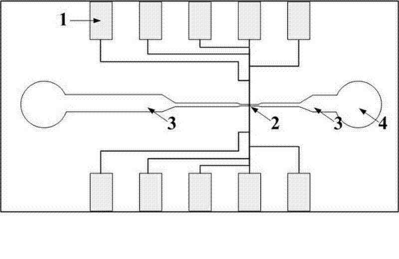
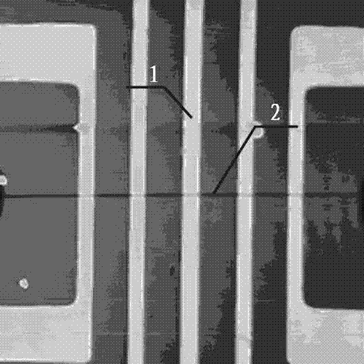
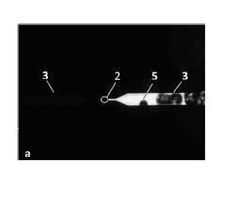
[0023] figure 1 It is the nanofluidic chip structure of the present invention, wherein the part indicated by 1 is an electrode, and 5 pairs of electrodes are designed on the chip, 2 is a nanotube processed by AFM, 3 is a micron tube, and 4 is a liquid storage pool.

[0024] The processing method is

[0025] 1) Design nanofluidic chips: design and process such figure 1 In the shown nanofluidic chip, the unconnected area in the middle of the micro-pipe 3 is the area to be processed, which is used for subsequent processing of the nano-pipe 2 by using the AFM processing method. In the chip structure, the electrode 1 can be used to detect and analyze the signal of the nano-object solution in the nano-pipe 2;

[0026] 2) AFM processing of nanopipes: by controlling the AFM probe to press into the surface of the chip to a certain depth and controlling the linear movement ...


PUM

PropertyMeasurementUnit
depthaaaaaaaaaa

Abstract

The invention discloses a nanofluidic chip, a processing method based on atomic force microscopy (AFM), and application. Each of two ends of the chip is provided with a liquid storage tank; each liquid storage tank is connected with a micron pipeline; a nano pipeline is arranged between two micron pipelines; and electrodes which are vertical to the pipelines are arranged on two sides of the nano pipeline. The nano pipeline which is communicated with the micron pipelines is processed by using an AFM probe. Certain voltage is applied between the liquid storage tanks of the chip, small voltage is applied to the electrodes on two sides of the pipelines simultaneously, and the change of a current signal is measured; and when an object flows through the electrodes in the nano pipeline, current changes, and signal detection can be used for analyzing the structural and physical characteristics of a nano material. Processing and signal detection methods for the nanofluidic chip can applied to low-cost and quick sequencing of deoxyribose nucleic acid (DNA) molecules.

Description

technical field [0001] The invention belongs to the field of nano-processing and nano-fluidic signal detection, and specifically relates to a method for processing a pipeline with nano-scale depth and width through AFM, and detecting the state of nano-objects flowing in the pipeline through transverse electrodes. Background technique [0002] Nanopipes refer to tiny pipes with at least one dimension at the nanoscale. Nanopipes have many advantages in the field of nanofluidic research. Because the size of nanotubes is on the nanoscale, it can be used to study novel physical properties of liquids and gases in such tiny tubes. Compared with nanopores, nanopipes have a longer one-dimensional scale, so that the liquid in the pipes can have a slower flow rate, thus improving the resolution of detection. At the same time, multiple detection points can be set on both sides of the nanopipe, which is helpful for high-sensitivity and multi-point detection of the characteristics of obj...

Claims


Application Information

Patent Timeline
Patent Type & Authority Applications(China)
IPC IPC(8): G01N27/403G01N27/26B82Y15/00B82Y40/00
Inventor 焦念东王志迁董再励
Owner SHENYANG INST OF AUTOMATION - CHINESE ACAD OF SCI
Why Eureka
Try Eureka