Developing method

A developing method and a developing method technology, applied in the developing field, can solve the problem of uneven graphic development and achieve the effect of improving uniformity

Inactive Publication Date: 2012-07-04
CSMC TECH FAB1 +1
View PDF5 Cites 9 Cited by
  • Summary
  • Abstract
  • Description
  • Claims
  • Application Information

AI Technical Summary

Problems solved by technology

[0006] In view of this, the present invention provides a development method, which can solve the problem of uneven development of graphics at different positions on the wafer after development, thereby improving the uniformity of critical dimensions of the device

Method used


Image

  • Developing method
  • Developing method
  • Developing method

Examples


Embodiment 1

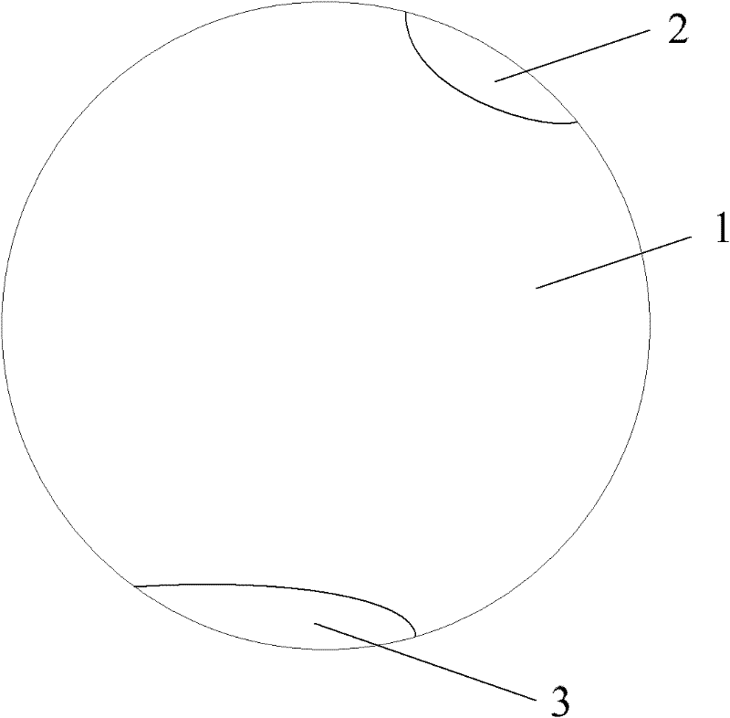
[0027] As mentioned in the background section, due to the high surface tension on the wafer surface, the developer at the edge of the wafer often shrinks due to the tension, which results in poor development of the edge of the wafer. Although the problem of poor development at the edge of the wafer can be solved by increasing the time of spraying the developer or increasing the dosage of the developer, it will also cause uneven development of graphics at different positions on the wafer, which in turn will worsen the uniformity of the critical dimensions of the device. .

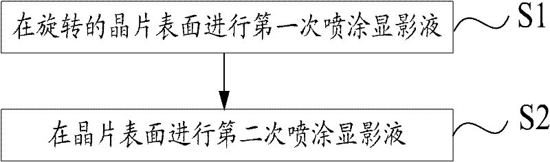
[0028] Based on this, the present invention provides a developing method, with reference to figure 2 , the method includes:

[0029] Step S1: Spraying developer solution on the surface of the rotating wafer for the first time.

[0030] In this step, after the wafer is placed on the vacuum chuck, the rotating motor connected to the vacuum chuck is controlled so that the vacuum chuck rotates together with t...

Embodiment 2

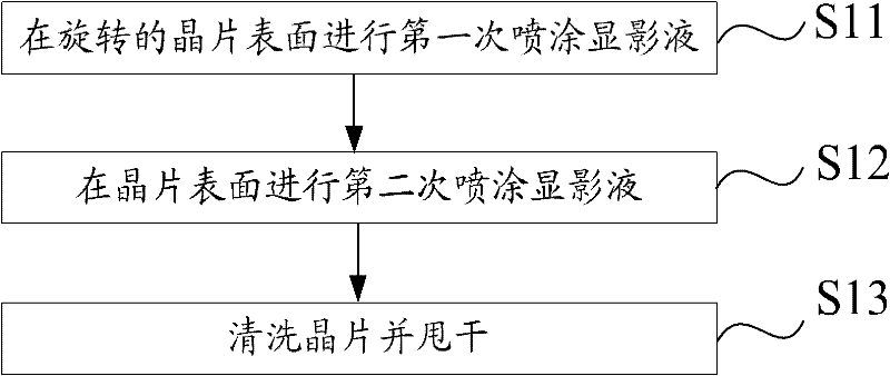
[0036] refer to image 3 , image 3 It is a flow chart of another developing method provided by an embodiment of the present invention, and the method specifically includes the following steps:

[0037] Step S11: Spraying developer on the surface of the rotating wafer for the first time.

[0038] Before this step, there is also a pretreatment step: cleaning the surface of the wafer with deionized water and drying it to ensure that the surface of the wafer is free from any impurities, pollutants or water sources. The wafers are then developed, which can be carried out on the same wafer track system.

[0039] After the wafer is pretreated, it is placed on the vacuum chuck in the automatic wafer track system to ensure that the wafer is placed stably and that the wafer and the vacuum chuck are relatively stationary. The vacuum chuck is connected to the rotating motor through a connecting rod (or pillar). By controlling whether the rotating motor is turned on, the vacuum chuck c...


PUM


Abstract

Embodiments of the invention disclose a developing method which comprises the following steps of: first spraying of a developer solution on a rotating wafer surface; second spraying of the developer solution on the wafer surface. According to the developing method provided by the invention, after the first spraying of the developer solution on the rotating wafer surface, the wafer surface is wetted uniformly, and thus the tension of the wafer surface is effectively reduced; therefore after the second spraying of the developer solution on the wafer surface, the developer solution sprayed for the second time is uniformly coated on the wafer; no poor development phenomenon occurs at the wafer edge, and the problem of non-uniform development of figures at different positions on the wafer is not caused; and thus the uniformity of device key dimensions is effectively improved.

Description

technical field [0001] The invention relates to the technical field of semiconductor manufacturing, and more specifically, to a developing method. Background technique [0002] In the semiconductor manufacturing process, the photolithography process generally includes the following steps: vapor phase bottom film formation, spin coating, soft baking, alignment and exposure, post-exposure baking, development, hard film baking and development inspection. Among them, developing is to generate a three-dimensional physical image in the photoresist, and this step determines whether the photoresist pattern is a true reproduction of the mask pattern. In the deep submicron semiconductor manufacturing process, development is a critical step for subsequent processing. [0003] The early developing method is to fix and immerse the wafer in the developing solution, and this method needs to consume a large amount of developing solution. In order to save developer, continuous spray develo...

Claims


Application Information

Patent Timeline
Patent Type & Authority Applications(China)
IPC IPC(8): G03F7/30
Inventor 胡骏李健
Owner CSMC TECH FAB1
Why Eureka
Try Eureka