

Transparent conductive film with enhanced thermal stability and application thereof
A technology of transparent conductive film and thermal stability, which is applied to the conductive layer, circuit, electrical components and other directions on the insulating carrier, and can solve the problem of poor thermal stability of OMO transparent conductive film
- Summary
- Abstract
- Description
- Claims
- Application Information
AI Technical Summary
Problems solved by technology
Method used
Image

Examples
Embodiment 1
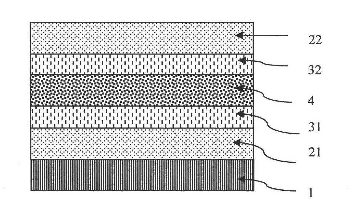
[0041] Such as figure 1 As shown, the transparent conductive film of this embodiment consists of a substrate 1, a first oxide layer 21, a first heavily doped layer 31, a metal layer 4, a second heavily doped layer 32, and a second oxide layer from bottom to top. Layer 22 composition. Wherein, the first oxide layer 21 is ZnO, the first heavily doped layer 31 is aluminum, the metal layer 4 is silver, the second heavily doped layer 32 is aluminum, and the second oxide layer 22 is ZnO. A single specific material is given here, without limiting the selection of other materials, but for better illustrating the present invention.
[0042] The electrical conductivity between the first oxide layer 21 and the metal layer 4 and between the second oxide layer 22 and the metal layer 4 is higher than the electrical conductivity inside the first oxide layer 21 and the second oxide layer 22 . For example, in the transparent conductive film with the above-mentioned structure of ZnO|Al|Ag|Al|...
Embodiment 2
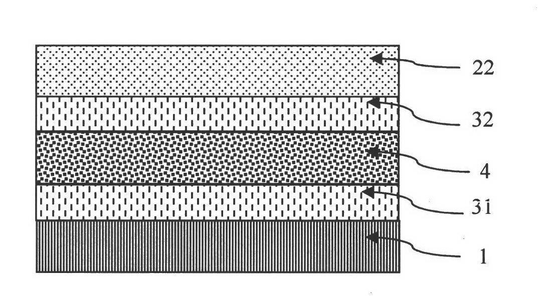
[0045] Such as figure 2 As shown, the transparent conductive film of this embodiment is composed of a substrate 1 , a first heavily doped layer 31 , a metal layer 4 , a second heavily doped layer 32 and a second oxide layer 22 from bottom to top. Wherein, the first heavily doped layer 31 is heavily aluminum-doped ZnO, the metal layer 4 is gold or silver, the second heavily doped layer 32 is heavily aluminum-doped ZnO, and the second oxide layer 22 is ZnO. A single specific material is given here, without limiting the selection of other materials, but for better illustrating the present invention. If the second oxide layer 22 is a degenerate semiconductor layer, such as ITO, AZO, and FTO, the transparent conductive film of this embodiment can be used as the cathode and anode of the photoelectric device.
Embodiment 3
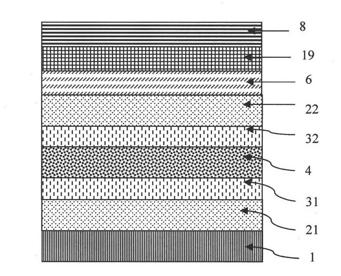
[0047] image 3 It is a schematic diagram of a transparent conductive film of the present invention made of specific materials and its application in OSC batteries. The specific materials listed in this embodiment do not limit the selection of other materials and film structures in the present invention, but are just for illustrating the present invention more clearly. The structure of the transparent conductive film and the OSC battery of this embodiment consists of the substrate 1 glass (thickness 1mm), the first oxide layer 21 AZO (thickness 10nm), and the first heavily doped layer 31 aluminum (thickness 0.8nm) from bottom to top. , metal layer 4 silver (thickness 12nm), second heavily doped layer 32 aluminum (thickness 0.8nm), second oxide layer 22 AZO (thickness 40nm), hole transport layer 6NiO (thickness 15nm), P3HT:PCBM Mixed layer 19 (mixed layer of polythiophene and fullerene) (thickness 200nm) and cathode 8 aluminum (thickness 150nm).
[0048] The square resistance o...
PUM
| Property | Measurement | Unit |
|---|---|---|
| Resistance | aaaaa | aaaaa |
| Sheet resistance | aaaaa | aaaaa |
| Thickness | aaaaa | aaaaa |
Abstract
Description
Claims
Application Information