High performance film-type touch sensor
a touch sensor, film-type technology, applied in the direction of instruments, superimposed coating processes, conductors, etc., can solve the problem of inevitable increase in resistance, and achieve the effect of high resolution, low resistance characteristics, and high performan
- Summary
- Abstract
- Description
- Claims
- Application Information
AI Technical Summary
Benefits of technology
Problems solved by technology
Method used
Image
Examples
first embodiment
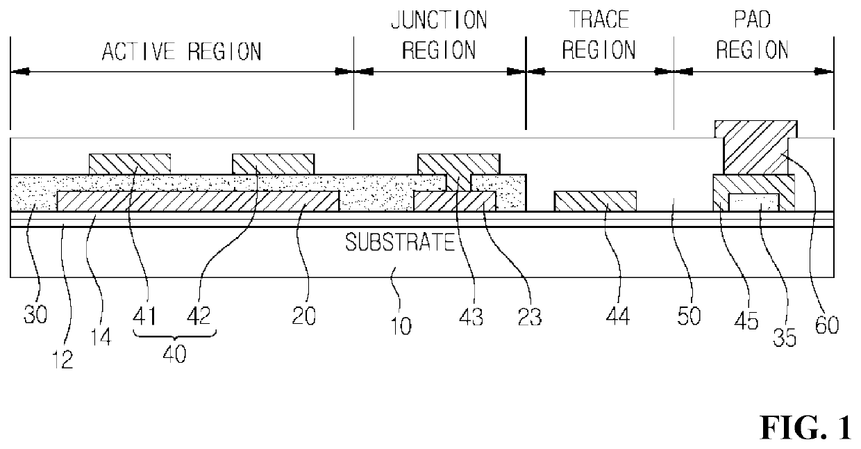
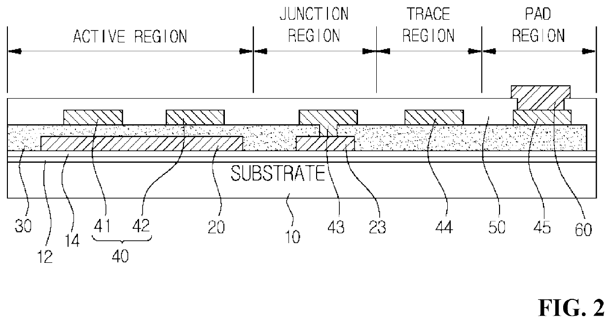
[0042]Referring to FIG. 1, the high performance touch sensor according to the present invention includes a substrate 10, a separation layer 12, an inner protective layer 14, a first sensing electrode 20, an insulating layer 30, a second sensing electrode 40, a pad electrode 45, a protective layer 50, and a pad protection electrode 60.
[0043]First, regions such as an active region AR, a junction region JR, a trace region TR, and a pad region PR, which functionally partition the high performance touch sensor according to the embodiments of the present invention, will be defined.
[0044]The active region AR is a region in which an image provided by a device coupled to the touch sensor is displayed as well as being a region in which a touch signal input from a user is detected. The active region AR is provided with a plurality of sensing electrode patterns formed in directions intersecting each other. Hereinafter, as will be described in detail, for example, the sensing electrode patterns ...
third embodiment
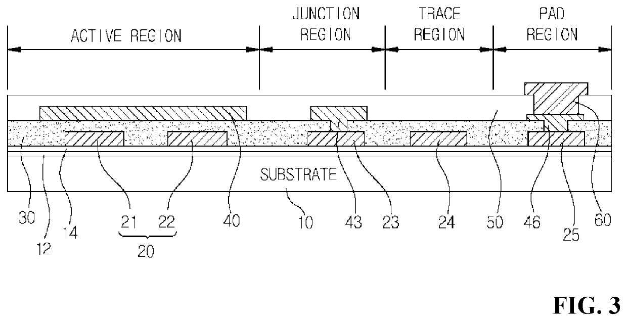
[0101]FIG. 3 is a view illustrating the high performance touch sensor according to the present invention.
[0102]Referring to FIG. 3, as opposed to the first and second embodiments, the high performance touch sensor according to the third embodiment of the present invention has a structure in which an electrode having a triple-layered structure is positioned at an upper side. That is, according to the third embodiment, a first sensing electrode 20 formed on a substrate 10 includes a metal pattern, and a second sensing electrode 40 formed on an insulating layer 30 has a triple-layered structure including a stacked metal oxide and thin film metal.
[0103]In the third embodiment of the present invention, such configurations applied to the first sensing electrode 20 and the second sensing electrode 40 overcome a contradictory relationship between resistance characteristics and optical characteristics and convert the contradictory relationship into a complementary relationship, thereby provi...
PUM
| Property | Measurement | Unit |
|---|---|---|
| width | aaaaa | aaaaa |
| width | aaaaa | aaaaa |
| line resistances | aaaaa | aaaaa |
Abstract
Description
Claims
Application Information


