Die bonder

A die-bonding machine and die-bonding technology, which is applied in the manufacture of semiconductor/solid-state devices, electrical components, circuits, etc., can solve the problems of difficulty in significantly increasing the operating frequency of the die-bonding head and high cost.

Active Publication Date: 2012-07-04
SUZHOU ACCURACY ASSEMBLY AUTOMATION CO LTD
View PDF5 Cites 52 Cited by
  • Summary
  • Abstract
  • Description
  • Claims
  • Application Information

AI Technical Summary

Problems solved by technology

Although the technical information of all crystal-bonding devices can be seen in the disclosed Chinese patent documents, for example, CN101281878B recommends that "crystal-bonding machine takes crystal arm drive control device" and CN10195838A provides "crystal-bonding machine head mechanism", etc., but Technical information on how to improve the die bonding efficiency of the die bonder is not disclosed
[0003]The factor that restricts the improvement of the die-bonding efficiency is mainly the working frequency of the die-bonding head. This is because the working stroke of the die-bonding swing arm of the die-bonding head is determined by The size of the wafer and the die-bonding object (lead frame or PCB board) is determined, so it is difficult to significantly increase the working frequency of the die-bonding head without changing the working stroke of the die-bonding arm, even through Corresponding technical means are used to increase the working frequency of the solid state head, and the price paid is extremely high.

Method used


Image

  • Die bonder
  • Die bonder
  • Die bonder

Examples


Embodiment 1

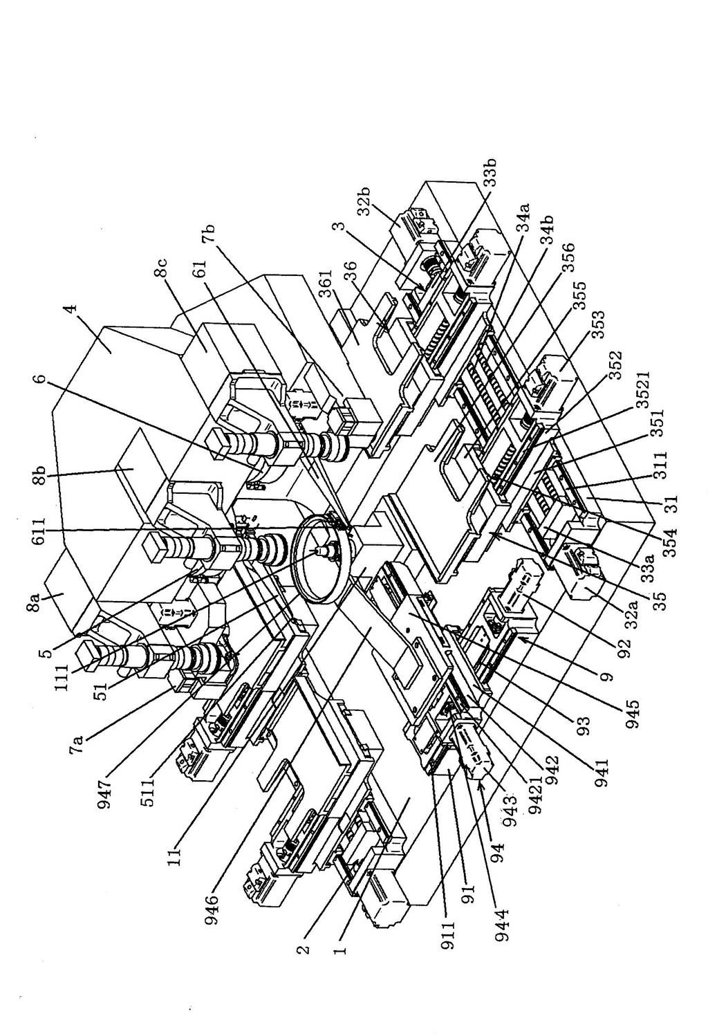
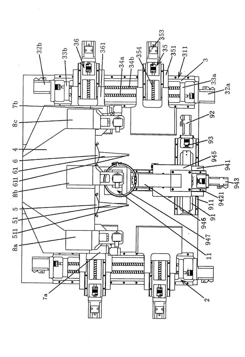
[0027] See Figure 1 to Figure 4 , a rectangular support platform 1 is provided, and a thimble mechanism 11 equipped with a thimble 111 is arranged at the central position of the support platform 1. The specific structure of the thimble mechanism 11 is preferably a cam structure to ensure the up and down of the thimble 111. vertical movement. at present figure 1 and figure 2 The position state shown is an example, a first die-bonding motion mechanism 2 is provided on the left side of the support platform 1, and a second crystal-bonding motion mechanism is provided on the right side and at a position corresponding to the first crystal-bonding motion mechanism 2 Mechanism 3, since the structures and working principles of the first and second crystal-bonding motion mechanisms 2 and 3 are the same, the applicant only elaborates on the second crystal-bonding motion mechanism 3 .

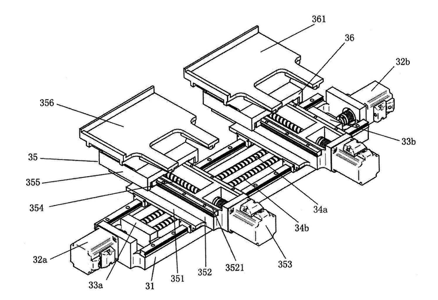
[0028] See the key points image 3 and combine figure 1 and figure 2 The preferred b...

Embodiment 2

[0041] please see Figure 6 and Figure 7 , only the first motor 32a on the first carrier moving device 35 and the second carrier moving device 36 of the second solid crystal moving mechanism 3, the second motor 32b, the first screw seat 33a, the second screw seat 33b, The first screw rod 34a, the second screw rod 34b use the first linear motor 37 with the first permanent magnet seat 371, the first permanent magnet 372 and the first coil 373 instead, and the third motor 353 and the third screw rod 354 are used instead The second linear motor 357 has a second permanent magnet seat 3571 , a second permanent magnet 3572 and a second coil 3573 , and the rest are the same as those described in Embodiment 1.


PUM


Abstract

The invention discloses a die bonder and belongs to the technical field of semiconductor packaging equipment. The die bonder comprises a supporting platform, a first die bonding movement mechanism, a second die bonding movement mechanism, a supporting vertical seat, a first die bonding head, a second die bonding head, a first dispensing module, a second dispensing module, a first camera module, a second camera module, a third camera module and a die taking movement mechanism, wherein a thimble mechanism which is provided with a thimble is arranged in the center of the supporting platform; the first die bonding movement mechanism is arranged on the left of the supporting platform; the second die bonding movement mechanism is arranged on the right of the supporting platform; the supporting vertical seat is fixed on the rear side of the supporting platform; the first die bonding head is provided with a first die bonding swinging arm; the second die bonding head is provided with a second die bonding swinging arm; the first die bonding head and the second die bonding head are arranged on the supporting vertical seat; the first dispensing module and the second dispensing module are arranged on the supporting vertical seat, the first dispensing module is arranged on the left of the supporting vertical seat, and the second dispensing module is arranged on the right of the supporting vertical seat; the first camera module, the second camera module and the third camera module are arranged on the supporting vertical seat; and the die taking movement mechanism is arranged on the front side of the supporting platform. The die bonder has the advantages that: economic cheapness is realized; and simplicity in the overall structure of the die bonder can be guaranteed.

Description

technical field [0001] The invention belongs to the technical field of semiconductor packaging equipment, in particular to a crystal bonder . Background technique [0002] As is well known in the industry, die bonding is an extremely important link in the packaging process of semiconductor devices such as ICs and LEDs. The process of solid crystal is: firstly, the glue dispensing mechanism (also called glue dispensing module) is used to dispense glue on the solid crystal station of the substrate, and then the solid crystal swing arm (also called solid crystal head) of the solid crystal mechanism (also called solid crystal head) Swing Arm) to remove the semiconductor die from the wafer, and then transfer it to the die-bonding station where the glue has been dispensed. Under the same die-bonding yield (quality) conditions, the die-bonding efficiency of the die-bonding machine is an important indicator for evaluating the performance of the die-bonding machine. Although the...

Claims


Application Information

Patent Timeline
Patent Type & Authority Applications(China)
IPC IPC(8): H01L21/67H01L33/00
Inventor 王敕杨宁
Owner SUZHOU ACCURACY ASSEMBLY AUTOMATION CO LTD
Why Eureka
Try Eureka