ESD (Electro-Static discharge) protection device with low trigger voltage and high balllast resistance for SCR (Silicon Controlled Rectifier)

A technology with low trigger voltage and device protection, applied in the field of electronics, can solve the problems of ESD performance degradation, uneven current, device overheating and burning, etc., to improve the ESD performance degradation, solve the effect of early device damage and high current discharge capability

Inactive Publication Date: 2012-07-04
UNIV OF ELECTRONICS SCI & TECH OF CHINA
View PDF6 Cites 15 Cited by
  • Summary
  • Abstract
  • Description
  • Claims
  • Application Information

AI Technical Summary

Problems solved by technology

This will bring the following problems: for a process with lightly doped drain (LDD) implantation, the LDD region with a shallower junction depth will cause a drop in ESD performance due to tip discharge; the concentration of avalanche current at the surface will cause serious local overheating, cause premature thermal damage to the device
In addition, in order to improve the operation speed, integration, and reliability of the internal circuits of CMOS ICs, modern advanced CMOS processes generally use metal silicide processes (Silicide) to reduce the series resistance of MOS devices at the drain and source terminals; but from From the perspective of ESD protection, the silicide process will reduce the internal ballast resistance of the device, which will cause uneven current, resulting in local overheating and burning of the device

Method used


Image

  • ESD (Electro-Static discharge) protection device with low trigger voltage and high balllast resistance for SCR (Silicon Controlled Rectifier)
  • ESD (Electro-Static discharge) protection device with low trigger voltage and high balllast resistance for SCR (Silicon Controlled Rectifier)
  • ESD (Electro-Static discharge) protection device with low trigger voltage and high balllast resistance for SCR (Silicon Controlled Rectifier)

Examples


specific Embodiment approach 1

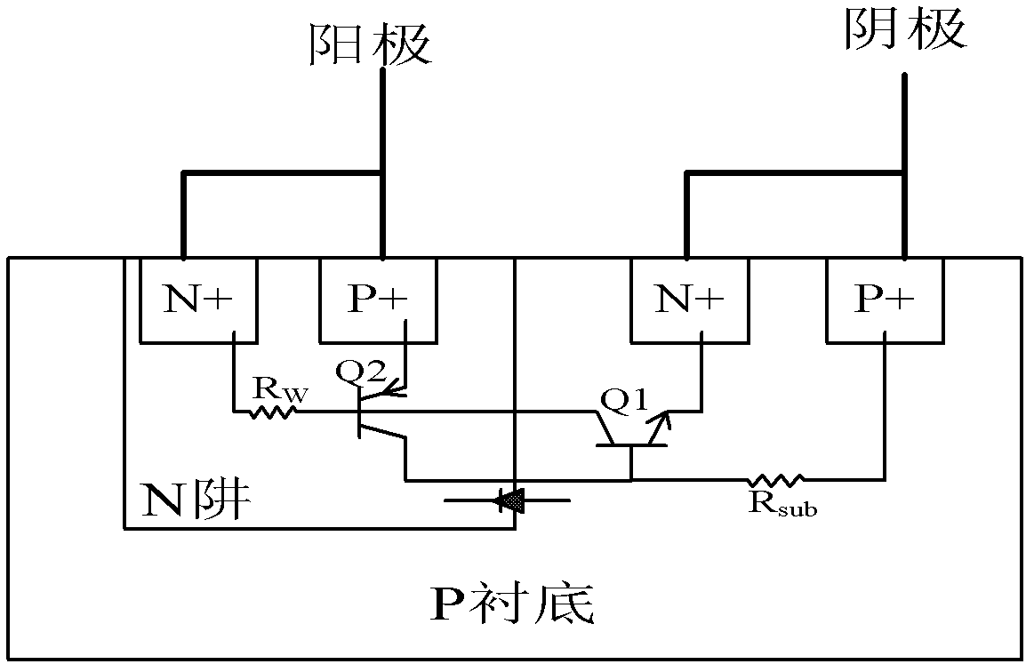
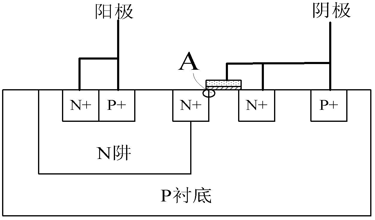
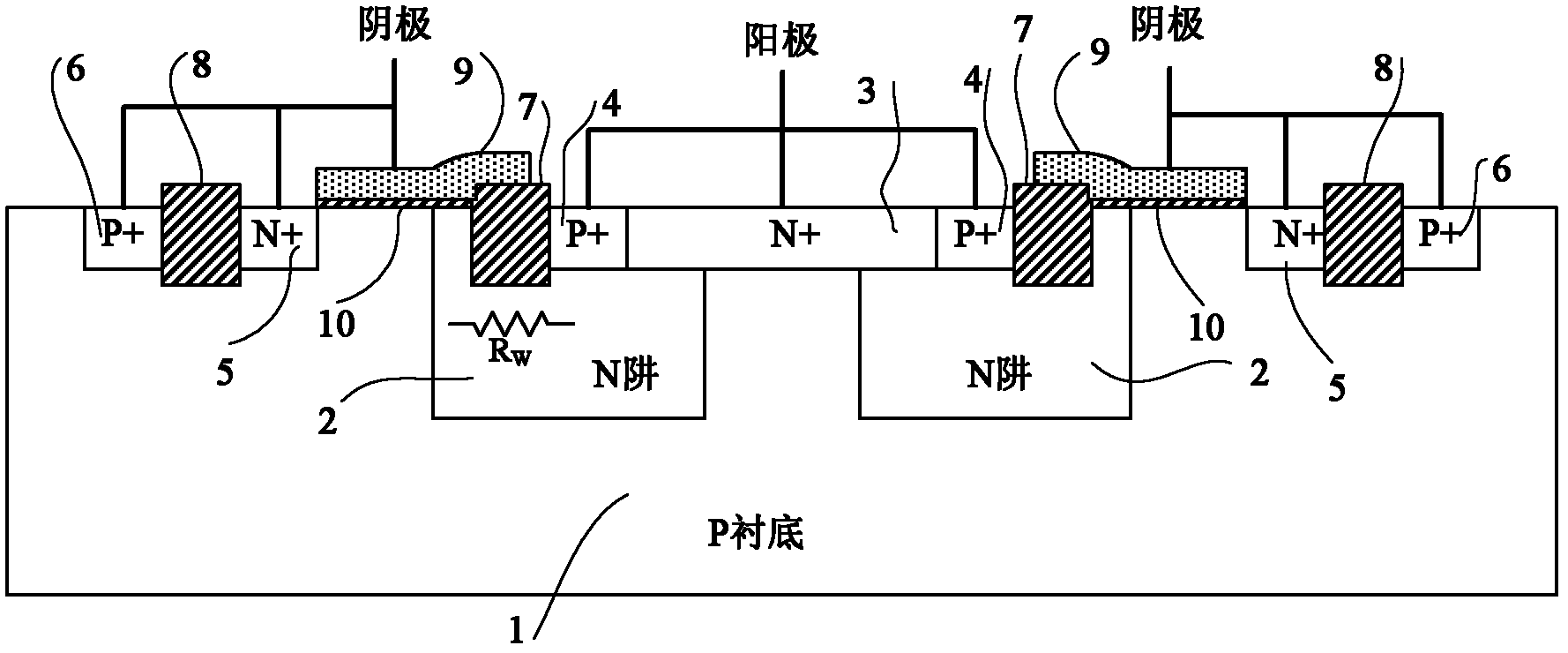
[0033] A SCR ESD protection device with low trigger voltage and high ballast resistance, such as image 3 As shown, it includes: P-type substrate 1, N-type well region 2 located on the P-type substrate, two N+ heavily doped regions 3 and 5, two P+ heavily doped regions 4 and 6, two shallow grooves Isolation regions 7 and 8 (Shallow Trench Isolation, STI for short) and a polysilicon gate region 9 . The N-type well region 2 is located at the top of the P-type substrate 1, the first P+ heavily doped region 4 and the first shallow trench isolation region 7 are located at the top of the N-type well region 2, and the first N+ heavily doped region 3 is connected to the P-type substrate. Type substrate 1 and the top of N-type well region 2 , the first P+ heavily doped region 4 is located between the first shallow trench isolation region 7 and the first N+ heavily doped region 3 . The second N+ heavily doped region 5, the second P+ heavily doped region 6 and the second shallow trench ...

specific Embodiment approach 2

[0034] A SCR ESD protection device with low trigger voltage and high ballast resistance, such as Figure 6 shown in image 3 On the basis of the shown structure, two P-type well regions 11 and 12 are added on the P-type substrate. The N-type well region 2 is sandwiched between two P-type well regions, the first N+ heavily doped region 3 spans the top of the N-type well region 2 and the first P-type well region 11, and the second N+ heavily doped region 5. The second P+ heavily doped region 6 and the second shallow trench isolation region 8 are located at the top of the second P-type well region 12 .

specific Embodiment approach 3

[0035] A SCR ESD protection device with low trigger voltage and high ballast resistance, such as Figure 7 shown in image 3 Based on the structure shown, a PBL buried layer region 15 is added in the P-type substrate 1 under the first N+ heavily doped region 3 .


PUM


Abstract

The invention discloses an ESD (Electro-Static discharge) protection device with low trigger voltage and high balllast resistance for an SCR (Silicon Controlled Rectifier), belonging to the technical field of electronics. By making use of the triggering of a heavily doped region and a substrate region in the vertical direction, the ESD protection device successfully transfers the avalanche breakdown from the surface of the device to the interior of the device, and with the addition of an STI (shallow trench isolation) region, the adverse effect of the silidide process is eliminated and the ballast resistance of the ESD protection device is effective improved.

Description

technical field [0001] The invention belongs to the field of electronic technology, and relates to the design technology of an electrostatic discharge (ElectroStatic Discharge, referred to as ESD) protection circuit of a semiconductor integrated circuit chip, especially a kind of silicon controlled rectifier (Silicon Controlled Rectifier, referred to as SCR) with low trigger voltage and high ballast resistance. ) ESD protection device. Background technique [0002] Electrostatic discharge is a common phenomenon in the process of manufacturing, producing, assembling, testing, storing, and transporting semiconductor devices or circuits. In the case of ESD, a large amount of charge will be transferred or transferred from the outside of the integrated circuit (IC) to the inside in a very short time, causing degradation of the performance of the integrated circuit or direct damage to the IC. In order to solve this problem, measures are usually taken in two aspects. The environme...

Claims


Application Information

Patent Timeline
Patent Type & Authority Applications(China)
IPC IPC(8): H01L29/87H01L29/06
CPCH01L29/87
Inventor 蒋苓利张波吴道训何川樊航
Owner UNIV OF ELECTRONICS SCI & TECH OF CHINA
Why Eureka
Try Eureka