Resin Encapsulation Apparatus And Resin Encapsulation Process

A resin sealing device and resin sealing technology, applied in the manufacture of electrical components, electrical solid devices, semiconductor/solid devices, etc., can solve the problems of semiconductor component damage, poor yield, etc., to achieve suppression of driving force, high productivity, and short forming cycle short effect

Inactive Publication Date: 2014-07-30
DAIICHI SEIKO CO LTD
View PDF1 Cites 0 Cited by
  • Summary
  • Abstract
  • Description
  • Claims
  • Application Information

AI Technical Summary

Problems solved by technology

In particular, if a crack occurs in the sealing resin 8 that is a molded product, the semiconductor element 9 or the Au wire 11 that is the object to be sealed may be damaged, and there is a problem that the yield is poor.

Method used


Image

  • Resin Encapsulation Apparatus And Resin Encapsulation Process
  • Resin Encapsulation Apparatus And Resin Encapsulation Process
  • Resin Encapsulation Apparatus And Resin Encapsulation Process

Examples


Embodiment Construction

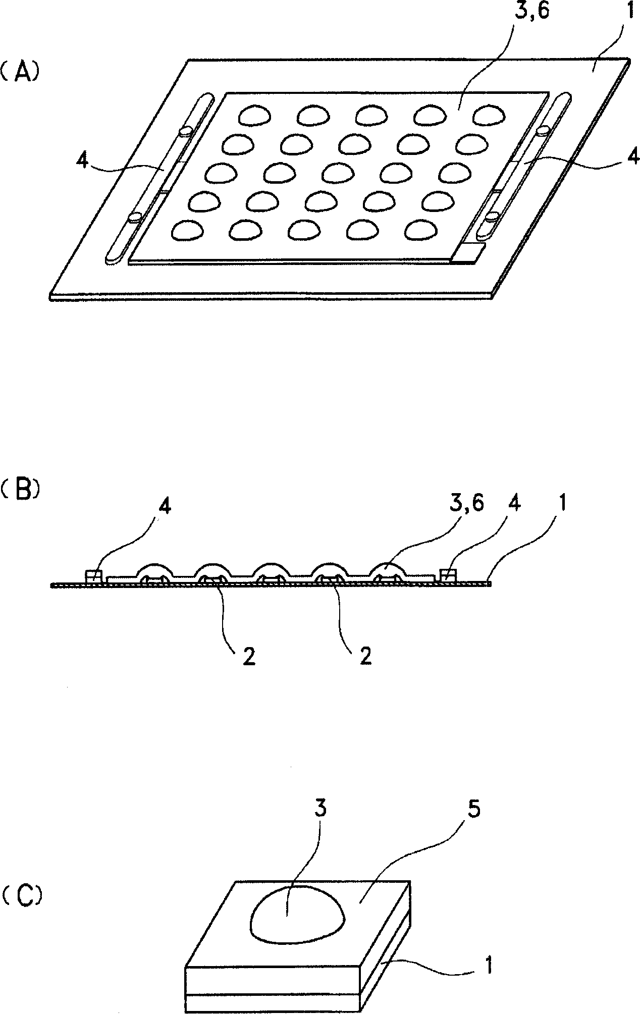
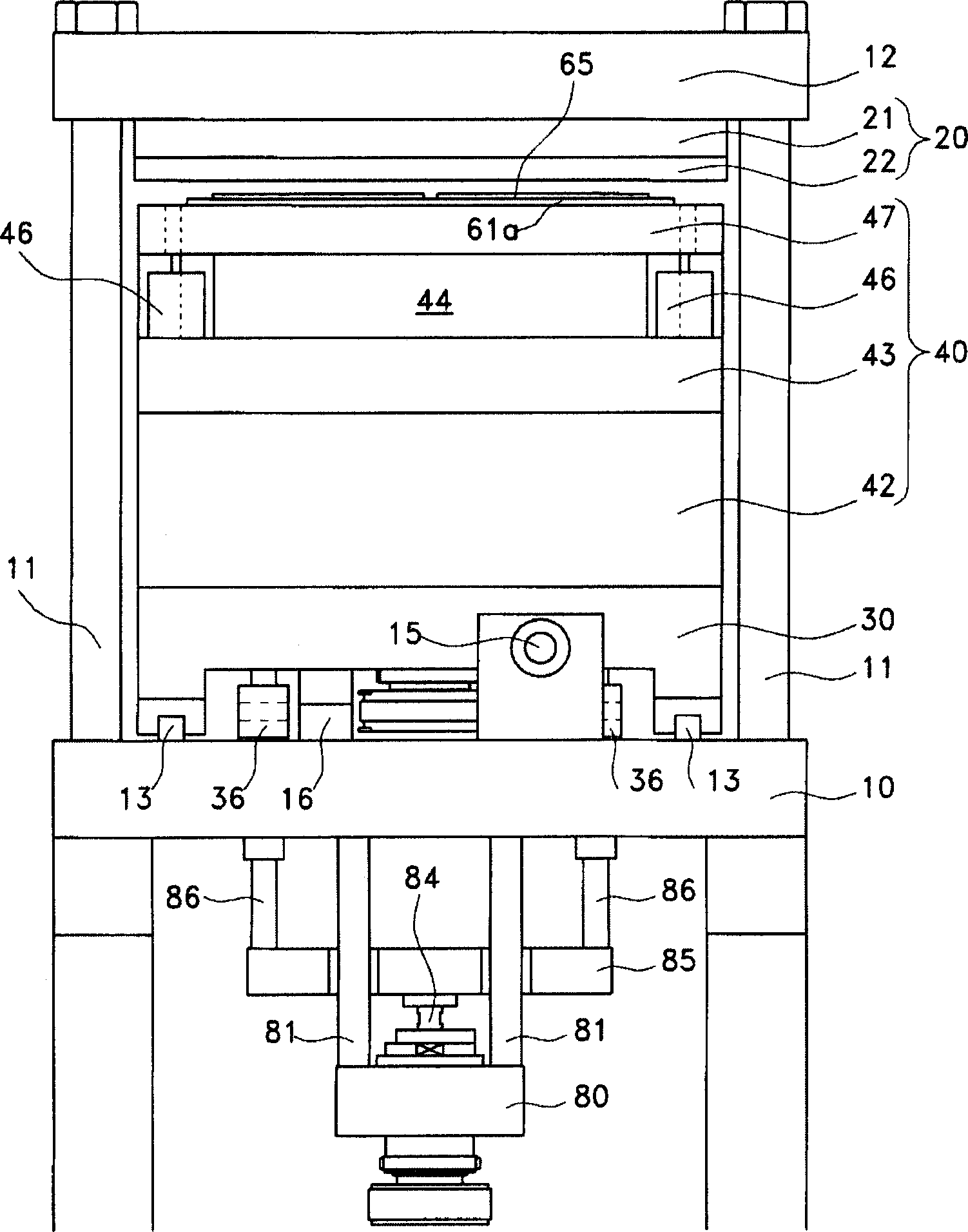
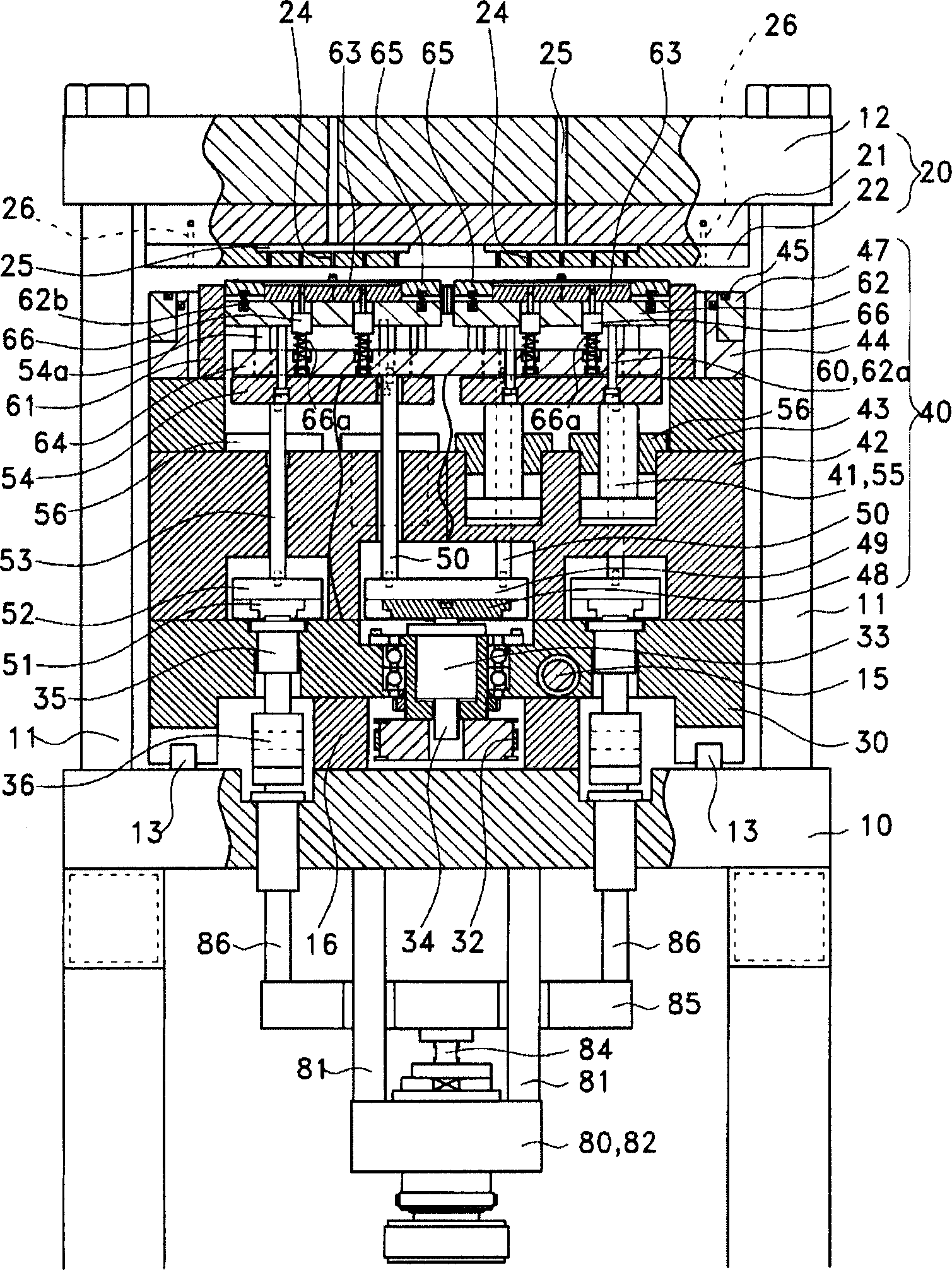
[0086] refer to Figure 1 to Figure 14 The accompanying drawings illustrate embodiments of the resin sealing device of the present invention.

[0087] like figure 1 (A), figure 1 As shown in (B), the resin sealing device of this embodiment is a device for resin sealing an optical semiconductor element 2, such as an LED, mounted on a ceramic substrate 1 printed with a conductive pattern at a predetermined pitch. on one side.

[0088] As the resin sealing material for resin-sealing LEDs according to the present embodiment, a silicone material excellent in heat resistance and translucency is used as a main raw material. This above-mentioned resin sealing material is not only a solid material called a tablet (tablet) that has been used all the time, but also can obtain a desired shape by injecting a liquid resin sealing material into a mold, heating it, and thermally curing it. shape. For example, in the present application, the molded product 3 including a surplus resin (Jap...


PUM


Abstract

A resin sealing device and resin sealing method capable of preventing damage to a substrate that may occur when a molded product is released from a mold and having a high yield rate. The molded product is formed by resin sealing a semiconductor element mounted on a substrate. The resin sealing device is composed of an upper mold assembly and a lower mold assembly, and the mold cavity body (63) at the forming position is moved up and down by the clamping mechanism, thereby utilizing the lower surface of the upper mold assembly and the cavity of the lower mold assembly The body (63) clamps and clamps the substrate (1) on which the electronic components are mounted, and the electronic components of the substrate (1) are immersed in the resin sealing material (9) supplied to the cavity to form a resin. Sealing, wherein the upper mold assembly has a holding mechanism capable of holding the substrate (1) on the lower surface, and the lower mold assembly is equipped with the cavity body (63) having the cavity portion on the upper surface And it can reciprocate along the bottom plate between the forming position and the standby position through the horizontal moving mechanism. Next, arrange frame guides (65) on at least two opposite sides of the outer periphery of the cavity (63), and use the frame guides (65) to lift the outer peripheral edge of the substrate (1) to demoulding.

Description

technical field [0001] The present invention relates to a resin sealing device and a resin sealing method for resin sealing semiconductor devices such as integrated circuits and optical semiconductor elements mounted on at least one surface of a substrate. Background technique [0002] Examples of substrates on which electronic components such as semiconductor elements mounted on the surface are resin-sealed include ceramic substrates made of ceramic materials with excellent heat dissipation properties and mounted with optoelectronic components such as LEDs and semiconductor lasers, power semiconductor elements, and the like. In addition, a resin sealing material is supplied to a cavity provided in a lower mold, the electronic components of the substrate are dipped and resin-sealed, and the resin-sealed molded product is sometimes released from the mold. For example, as in Patent Document 1 figure 1 As shown, the following structure is adopted: the resin sealing material 8 ...

Claims


Application Information

Patent Timeline
Patent Type & Authority Patents(China)
IPC IPC(8): B29C43/18B29C43/36H01L21/56
CPCH01L24/97H01L2224/48091H01L2224/45144H01L2924/14H01L2924/15787H01L2924/00014H01L2924/00H01L21/56H01L23/28
Inventor 田中裕一力丸诚
Owner DAIICHI SEIKO CO LTD
Why Eureka
Try Eureka