
Epitaxial substrate, semiconductor light emitting element using the same and manufacturing process

A technology for epitaxial substrates and light-emitting elements, which is applied in semiconductor/solid-state device manufacturing, semiconductor devices, electrical components, etc., can solve the problems of high manufacturing cost and slow production speed, and achieve low manufacturing cost, fast production, and excellent photoelectric efficiency. Effect

Active Publication Date: 2014-12-24
HANNSTAR DISPLAY NANJING
View PDF5 Cites 0 Cited by
  • Summary
  • Abstract
  • Description
  • Claims
  • Application Information

AI Technical Summary

Problems solved by technology

Clearly, prior art techniques for fabricating epitaxial substrates with patterned surfaces are costly and slow to manufacture

Method used


Image

  • Epitaxial substrate, semiconductor light emitting element using the same and manufacturing process
  • Epitaxial substrate, semiconductor light emitting element using the same and manufacturing process
  • Epitaxial substrate, semiconductor light emitting element using the same and manufacturing process

Examples


Embodiment Construction

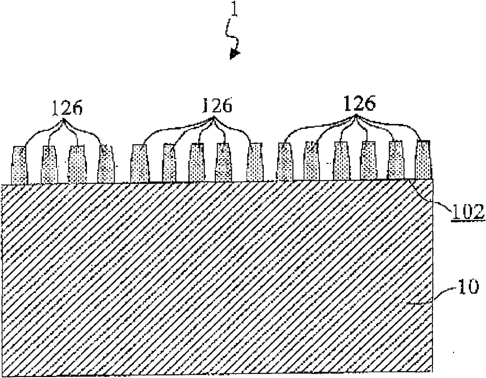
[0035] see figure 1 , figure 1 It is schematically drawn in a cross-sectional view on an epitaxial substrate 1 according to a preferred embodiment of the present invention. The epitaxy base 1 can be used for the epitaxy of a compound semiconductor material, for example, III-V compounds such as gallium nitride, aluminum gallium nitride, aluminum indium gallium nitride, or cadmium telluride, zinc oxide, zinc sulfide, etc. II-VI compounds.

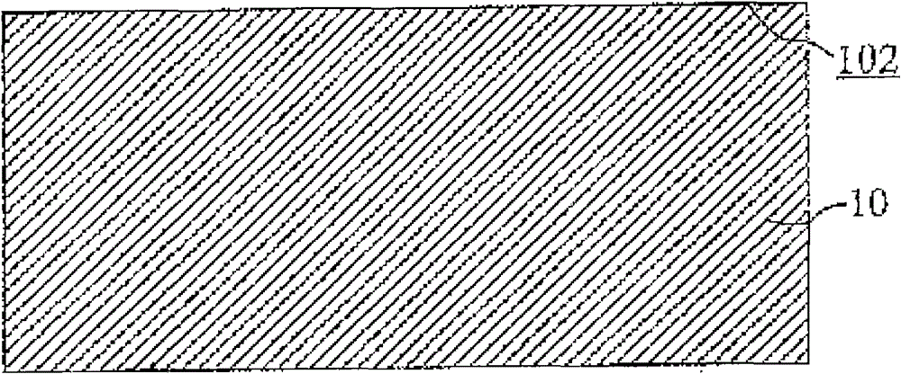
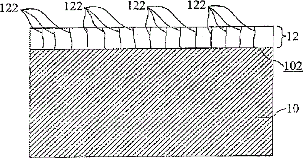
[0036] Such as figure 1 As shown, the epitaxial substrate 1 according to the present invention includes a crystal substrate 10 . The crystal substrate 10 has a crystal surface 102 .

[0037] In particular, a plurality of nanoscale pillars 126 are randomly arranged on the crystal surface 102 of the crystal substrate 10 . The plurality of nanoscale pillars 126 are formed by an oxide of a second material, and the second material is different from the first material. It should be noted that the surface of the epitaxial substrate 1 according...


PUM

PropertyMeasurementUnit
surface roughnessaaaaaaaaaa
thicknessaaaaaaaaaa
surface roughnessaaaaaaaaaa

Abstract

The invention provides an epitaxial substrate, a semiconductor light emitting element using the same and a manufacturing process. According to the invention, the epitaxial substrate comprises a crystal substrate. In particular, multiple nanoscale column bodies, which are dispersedly arranged, are arranged at the crystal surface of the crystal substrate. The multiple nanoscale column bodies are formed by oxides different from materials forming the substrate.

Description

1. Technical field [0001] The present invention relates to an epitaxial substrate, a semiconductor light-emitting element using the epitaxial substrate and a manufacturing method thereof, and in particular, the present invention relates to a hetero-nanorod An epitaxial substrate, a semiconductor light emitting device using the epitaxial substrate, and a manufacturing method thereof. 2. Background technology [0002] Compound semiconductor materials, such as: gallium nitride (GaN), aluminum potassium nitride (AlGaN), aluminum indium gallium nitride (AlInGaN) and other III-V compounds, as well as chromium telluride (CdTe), zinc oxide (ZnO), II-VI compounds such as zinc sulfide (ZnS) have been widely examined as substrate materials for electronic components, including but not limited to transistors, field emitters, and optoelectronic components. [0003] Taking GaN-based microelectronic devices as an example, a major problem in the manufacture of the GaN semiconductor layer is...

Claims


Application Information

Patent Timeline
Patent Type & Authority Patents(China)
IPC IPC(8): H01L21/02H01L21/20H01L29/06H01L33/02H01L33/20H01L33/00
Inventor 钱俊逸简宏吉杨昆霖徐文庆
Owner HANNSTAR DISPLAY NANJING
Learn More