Semiconductor device packaging method and semiconductor device package

A device packaging and semiconductor technology, applied in semiconductor devices, semiconductor/solid-state device parts, semiconductor/solid-state device manufacturing, etc., can solve problems such as increasing the size of discrete semiconductor devices

Inactive Publication Date: 2012-07-11
NXP BV
View PDF5 Cites 9 Cited by
  • Summary
  • Abstract
  • Description
  • Claims
  • Application Information

AI Technical Summary

Problems solved by technology

Placing the package in the resin mold layer can avoid this leakage current, but has the disadvantage that it significantly increases the size of the discrete semiconductor device package

Method used


Image

  • Semiconductor device packaging method and semiconductor device package
  • Semiconductor device packaging method and semiconductor device package
  • Semiconductor device packaging method and semiconductor device package

Examples


Embodiment Construction

[0026] It should be understood that the drawings are merely schematic and not drawn to scale. It should also be understood that like reference numbers are used throughout the drawings to indicate like or similar parts.

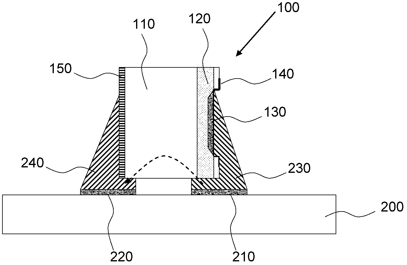
[0027] figure 1 A discrete semiconductor device package 100 is schematically depicted side mounted on a carrier 200 such as a PCB. The discrete semiconductor device package 100 includes a top contact 130 and a bottom contact 150, and has a wetting layer 140 applied to the top contact 130 to enhance its solderability (ie, its adhesion to solder materials). This wetting layer can be a plating layer or an under bump metallurgy (UBM). Suitable materials for wetting layer 140 are known to those skilled in the art. A further wetting layer (not shown) may be applied over the bottom contact 150 . Alternatively, the bottom contact 150 may be constructed of a material that has good adhesion properties with solder to be applied thereon.

[0028] A discrete semicondu...


PUM


Abstract

Disclosed is a method of manufacturing a discrete semiconductor device package (100), comprising providing a wafer comprising a plurality of semiconductor devices (50), each of said semiconductor devices comprising a substrate (110) having a top contact (130) and a bottom contact (150); partially sawing said wafer with a first sawing blade such that the semiconductor devices are partially separated from each other by respective incisions (20); lining said incisions with an electrically insulating film (160); and sawing through said incisions with a second sawing blade such that the semiconductor devices are fully separated from each other. A resulting discrete semiconductor device package (100) and a carrier (200) comprising such a discrete semiconductor device package (100) are also disclosed.

Description

technical field [0001] The present invention relates to a method of manufacturing discrete semiconductor device packages comprising providing a wafer having a plurality of semiconductor devices, each semiconductor device comprising a substrate having a top contact and a bottom contact. [0002] The invention further relates to a discrete semiconductor device package comprising a semiconductor device comprising a substrate having top contacts and bottom contacts. [0003] The invention still further relates to a carrier comprising such a discrete semiconductor device package. Background technique [0004] Discrete semiconductor devices such as diodes are typically marketed in packaged form. The package protects the discrete semiconductor device from accidental damage and provides contacts to enable integration of the discrete semiconductor device into a larger electronic device, for example by mounting the discrete semiconductor device on a printed circuit board (PCB). Sinc...

Claims


Application Information

Patent Timeline
Patent Type & Authority Applications(China)
IPC IPC(8): H01L23/00
CPCH01L23/3178H01L2224/04026H01L2924/1304H01L2224/26145H01L2224/0558H01L2224/03464H01L2224/05666H01L2924/10155H01L2224/06181H01L2924/12036H01L21/78H01L2224/05655H01L2224/94H01L23/3171H01L2224/32225H01L2224/27013H01L2224/03H01L2924/01028H01L2924/01047H01L2924/01079H01L2924/01046
Inventor 斯文·沃尔兹克洛尔夫·安科约科伯·格罗恩休斯保罗·戴克斯特拉埃米尔·德·布鲁因洛尔夫·布莱纳
Owner NXP BV
Why Eureka
Try Eureka