Process for laminating printed circuit board (PCB) with buried/blind via structure

A PCB board and buried blind hole technology, which is applied in the lamination process of PCB boards, can solve the problems of large amount of misalignment between layers, affect welding strength, and damage the flatness of steel plates, etc., so as to reduce the amount of misalignment between layers and improve work efficiency. , Reduce the effect of work intensity

Inactive Publication Date: 2012-07-11
SIHUI FUJI ELECTRONICS TECH
View PDF4 Cites 16 Cited by
  • Summary
  • Abstract
  • Description
  • Claims
  • Application Information

AI Technical Summary

Problems solved by technology

At present, when the PCB board with buried blind hole structure is manufactured in multi-layer lamination, a via hole is drilled on the core board, and a prepreg is placed between the two core boards. During the lamination process, the resin on the prepreg will be squeezed into the core. In the via hole on the board, after continuing to press, the resin in the via hole will flow out of the via hole and stick to the surface of the core board. It needs to be grinded many times by a grinder to eliminate the sticking on the surface of the core board. During the grinding process, the core board and the copper foil on its surface are easily damaged, so that it is scrapped, and due to mechanical equipment and human factors, sometimes it cannot be ground cleanly, which affects the subsequent use performance
[0003] In addition, during processing, the current practice is generally to rivet the two core plates with rivets first. During the processing, the rivets are basically in hard contact with the tool steel plate, and the riveting point is also the stress point, which will easily cause the rivet to be deformed by force and cause layer damage. misalignment
Since the riveting point

Method used


Image

  • Process for laminating printed circuit board (PCB) with buried/blind via structure
  • Process for laminating printed circuit board (PCB) with buried/blind via structure

Examples


Embodiment 1

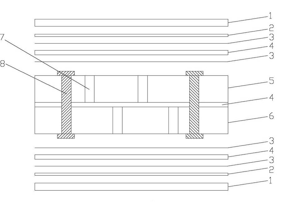
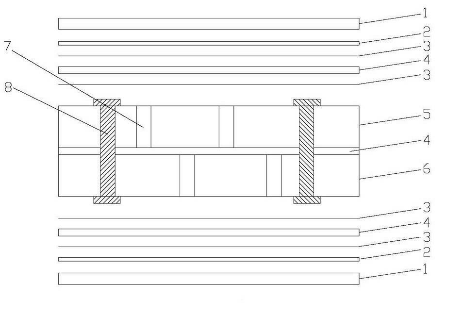
[0020] Embodiment 1, the upper core board 5 and the lower core board 6 are two-layer boards that have been drilled, electroplated and pattern transferred, and a release film 3 is sequentially laid on the upper surface of the upper core board 5 from bottom to top , a prepreg 4, a release film 3, an aluminum sheet 2, a mirror steel plate 1, a release film 3, a prepreg 4, One piece of release film 3, one piece of aluminum sheet 2, one piece of mirror steel plate 1, the thickness of release film 3 is 0.03mm, the thickness of prepreg 4 is 0.16mm, and the thickness of aluminum sheet 2 is 0.15mm. After pressing, it is For 4-layer boards, the prepreg changes from a semi-cured state to a fully cured state to become a cured sheet, remove the aluminum sheet, and remove the prepreg attached to the release film, and then undergo subsequent processing to form a 4-layer structure with buried blind holes PCB board.

Embodiment 2

[0021] Embodiment 2, the upper core board 5 and the lower core board 6 are four-layer boards that have been drilled, electroplated and pattern transferred, and a release film 3 is sequentially laid on the upper surface of the upper core board 5 from bottom to top , a prepreg 4, a release film 3, an aluminum sheet 2, a mirror steel plate 1, a release film 3, a prepreg 4, A release film 3, an aluminum sheet 2, and a mirror steel plate 1, the release film 3 has a thickness of 0.04mm, the prepreg 4 has a thickness of 0.18mm, and the aluminum sheet 2 has a thickness of 0.18mm. After pressing, it becomes an eight-layer board. The prepreg changes from a semi-cured state to a fully cured state to become a cured sheet. The aluminum sheet is removed, and the prepreg attached to the release film is removed. After subsequent processing, an eight-layer structure is formed. hole PCB board.

Embodiment 3

[0022] Embodiment 3, both the upper core board 5 and the lower core board 6 are eight-layer boards that have been drilled, electroplated and pattern transferred, and a release film 3 is sequentially laid on the upper surface of the upper core board 5 from bottom to top , a prepreg 4, a release film 3, an aluminum sheet 2, a mirror steel plate 1, a release film 3, a prepreg 4, One piece of release film 3, one piece of aluminum sheet 2, one piece of mirror steel plate 1, the thickness of release film 3 is 0.05mm, the thickness of prepreg 4 is 0.19mm, the thickness of aluminum sheet 2 is 0.20mm, after pressing For 16-layer boards, the prepreg changes from a semi-cured state to a fully cured state to become a cured sheet, remove the aluminum sheet, and remove the prepreg attached to the release film, and then undergo subsequent processing to form a 16-layer buried blind hole PCB board.

[0023] The invention utilizes aluminum sheet, prepreg and release film as auxiliary pressing m...


PUM

PropertyMeasurementUnit
Thicknessaaaaaaaaaa
Thicknessaaaaaaaaaa
Thicknessaaaaaaaaaa

Abstract

The invention discloses a process for laminating a printed circuit board (PCB) with a buried/blind via structure. The process comprises the following steps of: (1) drilling via holes on an upper core board and a lower core board to be laminated, electroplating the via holes to transfer patterns, arranging a prepreg between the upper core board and the lower core board, and connecting the upper core board, the prepreg and the lower core board through rivets; (2) laying a release film, the prepreg, the release film, an aluminum sheet and laminated steel on an upper surface of the upper core board in turn from bottom to top, and laying the release film, the prepreg, the release film, the aluminum sheet and the laminated steel on a lower surface of the lower core board in turn from top to bottom; (3) laminating; and (4) removing the aluminum sheet, and detaching the prepreg to which the release film is attached so as to obtain the finished product. The process is convenient to operate, the labor cost is saved, the processing time is shortened, the working efficiency is improved, the labor intensity is reduced, and the yield of the product is improved.

Description

technical field [0001] The invention relates to a pressing process of a PCB board, in particular to a pressing process of a PCB board with a buried blind hole structure. Background technique [0002] With the advancement of science and technology, the number of layers of PCB boards is increasing, and the structure is becoming more and more complex. PCB boards are formed by laminating core boards and semi-cured laminates, and multilayer boards are composed of multiple core boards. . At present, when the PCB board with buried blind hole structure is manufactured in multi-layer lamination, a via hole is drilled on the core board, and a prepreg is placed between the two core boards. During the lamination process, the resin on the prepreg will be squeezed into the core. In the via hole on the board, after continuing to press, the resin in the via hole will flow out of the via hole and stick to the surface of the core board. It needs to be grinded many times by a grinder to elim...

Claims


Application Information

Patent Timeline
IPC IPC(8): H05K3/46
Inventor 王爱军刘天明
Owner SIHUI FUJI ELECTRONICS TECH
Why Eureka
Try Eureka