System and method for carrying out light/electrical/thermal ageing comprehensive testing on light-emitting diodes

A light-emitting diode and comprehensive detection technology, which is applied in the direction of testing optical properties, single semiconductor device testing, etc., can solve the problems that in-situ detection cannot be implemented

Active Publication Date: 2012-07-25
INST OF SEMICONDUCTORS - CHINESE ACAD OF SCI
View PDF8 Cites 36 Cited by
  • Summary
  • Abstract
  • Description
  • Claims
  • Application Information

AI Technical Summary

Problems solved by technology

[0007] In addition, although there are test devices for measuring light, electricity, and heat of LEDs in the domestic and foreign markets, and there are also aging devices for LEDs, but in general, they are performed independently on different operating platforms, requiring operators to interrupt

Method used


Image

  • System and method for carrying out light/electrical/thermal ageing comprehensive testing on light-emitting diodes
  • System and method for carrying out light/electrical/thermal ageing comprehensive testing on light-emitting diodes
  • System and method for carrying out light/electrical/thermal ageing comprehensive testing on light-emitting diodes

Examples


Embodiment Construction

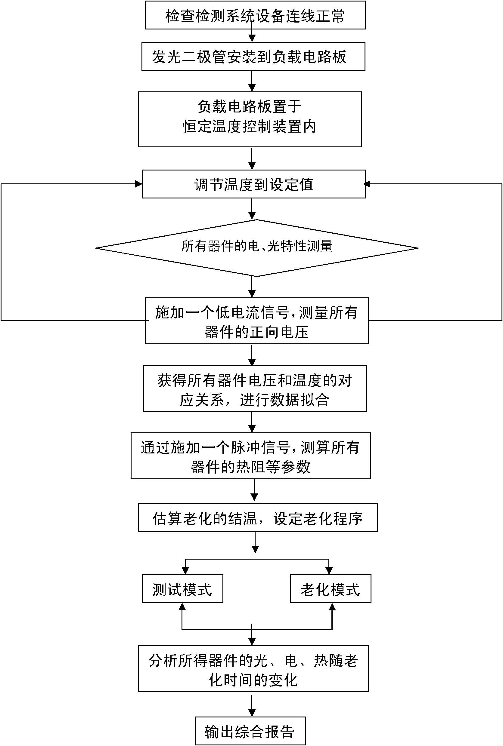
[0027] In order to make the object, technical solution and advantages of the present invention clearer, the present invention will be described in further detail below in conjunction with specific embodiments and with reference to the accompanying drawings.

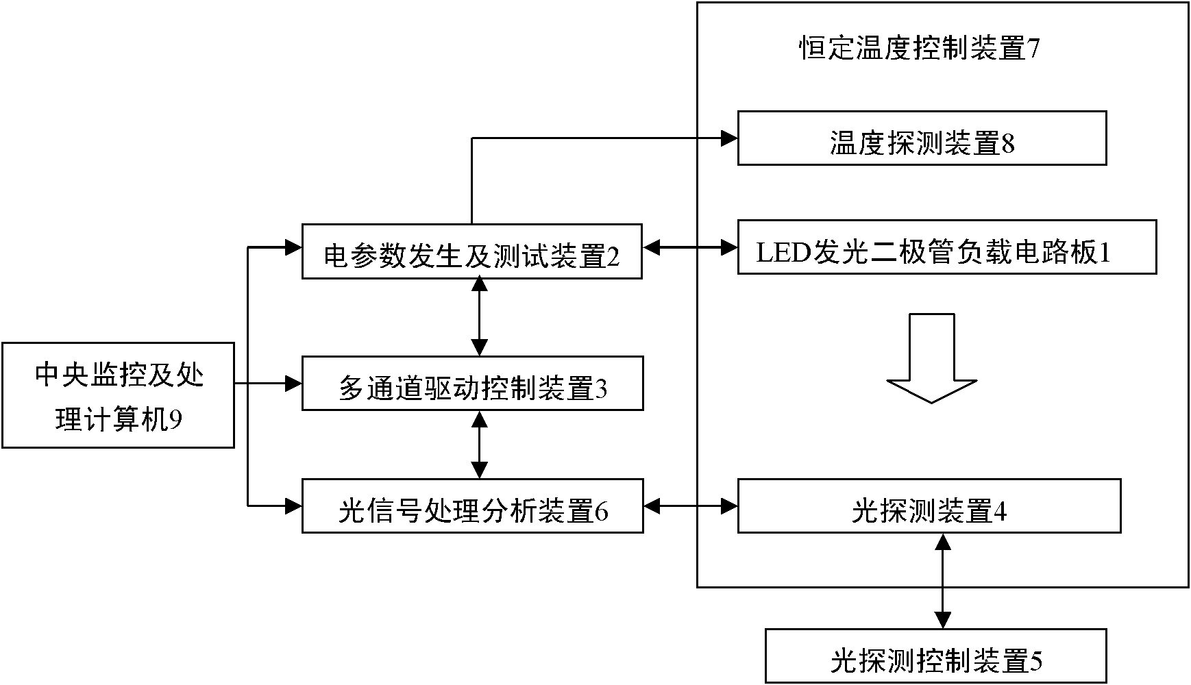
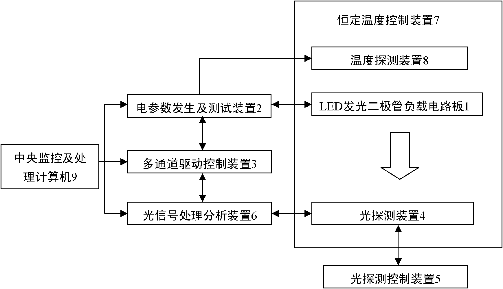
[0028] The present invention detects the properties of light, electricity, heat and the like of the light emitting diodes in situ during the aging process of a plurality of light emitting diodes. In the present invention, a load circuit board loaded with a single or multiple light-emitting diodes is placed in a constant temperature control device, and the electric parameter generation and testing device not only drives the LED to emit light, but also can measure the current and voltage scanning characteristics of the light-emitting diode; different LED channels The switching of the multi-channel drive control device is used to complete; the light signal emitted by the light-emitting diode is received by a light detection d...


PUM


Abstract

The invention discloses a system and method for carrying out in-situ light/electrical/thermal comprehensive testing on a plurality of light-emitting diode devices while carrying out accelerated aging on the light-emitting diode devices. The detection system comprises a light-emitting diode loading circuit board (1), an electrical parameter generating and testing device (2), a multi-channel drive control device (3), a light detection device (4), a light detection control device (5), a light signal processing analysis device (6), a constant temperature control device (7), a temperature detection device (8) and a central monitoring and processing computer (9). By using the system and method disclosed by the invention, a plurality of light-emitting diodes can be subjected to accelerated aging, and the electrical, optical and thermal properties of each light-emitting diode device can be tested one by one through setting time nodes by the computer so as to comprehensively understand the overall physical properties of the light-emitting diode (LED) devices.

Description

technical field [0001] The invention belongs to the technical field of detection of semiconductor light-emitting diodes, and in particular relates to a system and method for comprehensive detection of photoelectric and thermal aging of light-emitting diodes. Background technique [0002] A light emitting diode (light emitting diode, LED) is a solid light emitting device using a semiconductor chip as a light emitting material. The semiconductor material is used to form a PN junction, and in the case of an external electric field, the injected electron-hole recombination emits light, and directly converts electrical energy into light energy. Its luminous color varies with the semiconductor composition used. [0003] In 1907, Henry Joseph Round successfully prepared the first light-emitting diode. Subsequently, after about half a century of development, the materials of light-emitting diodes have experienced SiC, III-V compounds, etc., and the wavelength range covers infrared...

Claims


Application Information

Patent Timeline
IPC IPC(8): G01R31/26G01M11/02
Inventor 赵丽霞杨华王军喜王国宏曾一平李晋闽
Owner INST OF SEMICONDUCTORS - CHINESE ACAD OF SCI
Why Eureka
Try Eureka