Liquid crystal panel, liquid crystal module and method for clarifying reasons resulting in poor screen images thereof

A liquid crystal panel and circuit board technology, applied in nonlinear optics, instruments, optics, etc., can solve problems such as testing, affecting product production, and inability to guarantee product quality, and achieve the effect of reducing costs and improving accuracy

Active Publication Date: 2012-08-01
SHENZHEN CHINA STAR OPTOELECTRONICS TECH CO LTD
View PDF6 Cites 45 Cited by
  • Summary
  • Abstract
  • Description
  • Claims
  • Application Information

AI Technical Summary

Problems solved by technology

When the product screen is found to be defective, it is necessary to clarify whether the cause of the defect is caused by the Cell process or the Module process.
However, the test lead of the shorting bar has been cut off in the laser machine during the Cell process, and the test lead of the shorting bar in the Cell process cannot be used again to test the picture, so it is diffic

Method used


Image

  • Liquid crystal panel, liquid crystal module and method for clarifying reasons resulting in poor screen images thereof
  • Liquid crystal panel, liquid crystal module and method for clarifying reasons resulting in poor screen images thereof
  • Liquid crystal panel, liquid crystal module and method for clarifying reasons resulting in poor screen images thereof

Examples


Embodiment Construction

[0025] The present invention will be described in detail below in conjunction with the accompanying drawings and embodiments.

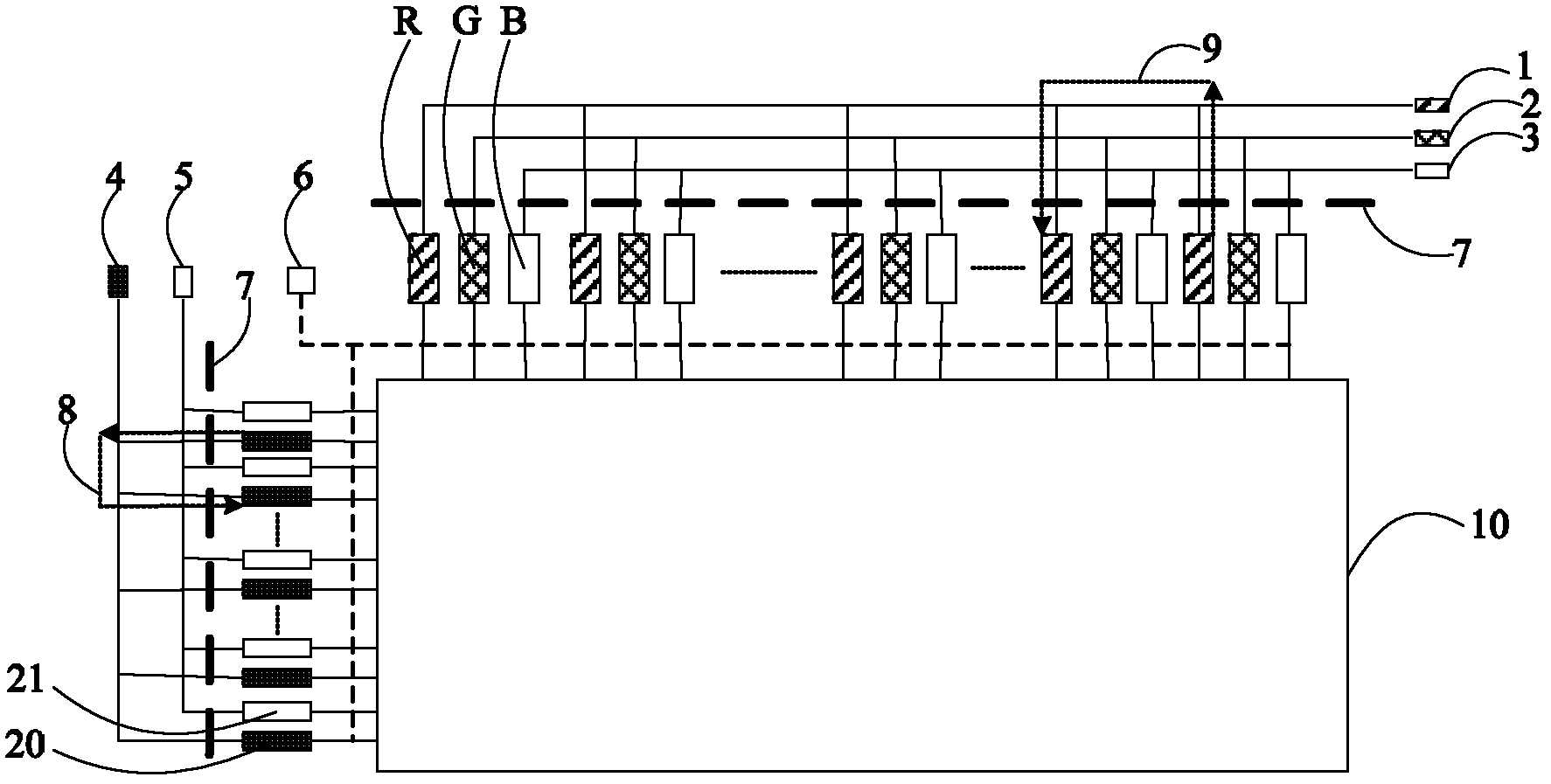
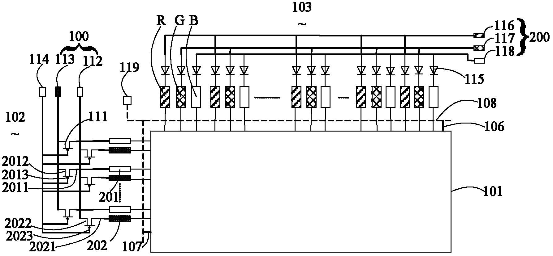
[0026] refer to figure 2 , figure 2 It is a structural schematic diagram of an embodiment of the liquid crystal panel of the present invention. The liquid crystal panel of the present invention includes a pixel area 101 and a testing short bar area (not shown) disposed on the periphery of the pixel area 101 .

[0027] Wherein, the pixel area 101 is provided with a plurality of data signal lines, a plurality of scanning signal lines and common electrodes (both not shown in the figure). The plurality of data signal lines, the plurality of scanning signal lines and the common electrodes extend out of the shorting bar area, such as figure 2 As shown, the multiple data signal lines include multiple R signal lines, multiple G signal lines, and multiple B signal lines, and the multiple scanning signal lines include multiple scanning odd lines 201 and m...


PUM


Abstract

The invention discloses a liquid crystal panel which comprises a pixel area and a test short-circuiting bar area arranged at the periphery of the pixel area, wherein the short-circuiting bar area is provided with a plurality of first switch circuits, a plurality of scanning signal test points, a public electrode test point, a plurality of first unidirectional circuits or second switch circuits, and a plurality of data signal test points; scanning signal lines are connected with the scanning signal test points by the first switch circuits; data signal lines are connected with the data signal test points by the first unidirectional circuits or second switch circuits; and a public electrode is connected with a public electrode test point. The invention also discloses a method for clarifying reasons resulting in poor screen images of a liquid crystal module. Through the way, by using the liquid crystal panel disclosed by the invention, an effect of saving cutting equipment and a process of cutting a test lead of the short-circuiting bar area in the manufacturing process of assembly can be achieved, so that in the subsequent production stages after the manufacturing process of assembly, the test lead of the short-circuiting bar area can continue to be used for carrying out screen image detection, thereby improving the test accuracy of screen images.

Description

technical field [0001] The invention relates to the field of liquid crystal display, in particular to a liquid crystal panel, a liquid crystal module and a method for clarifying the cause of its defective picture. Background technique [0002] Due to the advantages of low radiation, low power consumption and light weight of liquid crystal displays, more and more electronic products use liquid crystal displays as their display panels, such as mobile phones, computers and televisions. Wherein, a TFT (Thin Film Transistor, Thin Film Field Effect Transistor) liquid crystal display is one of the liquid crystal displays. [0003] The working principle of the thin film field effect transistor liquid crystal display is: through the appropriate voltage loading on the liquid crystal layer combined with the array glass substrate and the color filter glass substrate, the liquid crystal molecules in the liquid crystal layer are deflected under the action of voltage, and controlled by dif...

Claims


Application Information

Patent Timeline
IPC IPC(8): G02F1/13G02F1/1362G02F1/1368
CPCG02F2001/136254G09G3/006G02F1/1362G02F1/1309G02F1/1345G09G3/36G02F1/136254
Inventor 邓明锋蔡荣茂廖学士庄益壮文松贤
Owner SHENZHEN CHINA STAR OPTOELECTRONICS TECH CO LTD
Why Eureka
Try Eureka