

Semiconductor packaging structure and packaging method thereof
A packaging structure and semiconductor technology, which is applied in the direction of semiconductor devices, semiconductor/solid-state device manufacturing, semiconductor/solid-state device components, etc., can solve the problems of high cost, complicated process, and the thickness of the adapter board can not be too thick, so as to reduce the production cost , The effect of reducing the difficulty of the process
- Summary
- Abstract
- Description
- Claims
- Application Information
AI Technical Summary
Problems solved by technology
Method used
Image

Examples
specific Embodiment approach
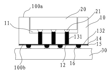
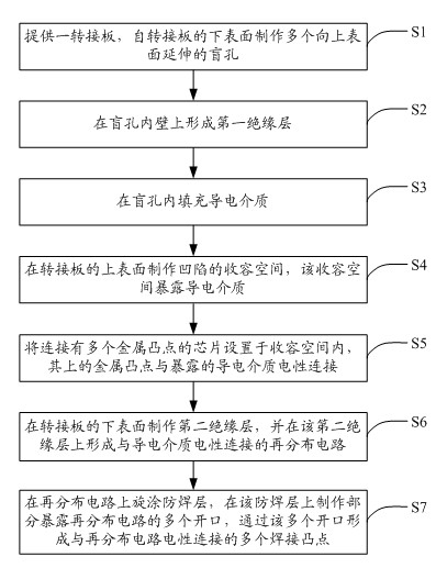
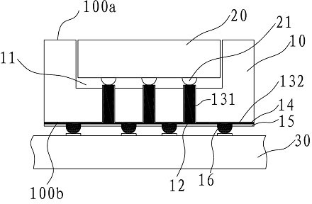
[0045] With reference figure 2 , to introduce a specific implementation of the semiconductor packaging method of the present invention, the method specifically includes the following steps:
[0046]S1. Provide an adapter plate 10, which includes an upper surface 100a and a lower surface opposite to the upper surface 100a. The material of the adapter plate 10 can be selected from silicon, glass and other semiconductor process well-known to those of ordinary skill in the art. Substrate material, on the lower surface 100b of the adapter plate 10, form a plurality of blind holes extending to the upper surface 100a of the adapter plate to a certain depth, specifically: spin coat a layer of photoresist on the lower surface 100b of the adapter plate 10, and The photoresist-coated side is exposed through a pre-designed mask plate (not shown), and then the exposed photoresist is washed away by developing to expose part of the interposer 10 area; Etching or wet etching technology will...
PUM
 Abstract
Description
Claims
Application Information