Image sensor packaging method

An image sensor and packaging method technology, applied in the semiconductor field, can solve the problems of reducing the sensitivity of the image sensor, reducing the incident light intensity of the image sensor, etc.

Active Publication Date: 2012-08-01
GALAXYCORE SHANGHAI
View PDF8 Cites 21 Cited by
  • Summary
  • Abstract
  • Description
  • Claims
  • Application Information

AI Technical Summary

Problems solved by technology

However, the glass covered on the photosensitive surface will absorb the light incident on the image sensor chip, resulting in a decrease in the incident light intensity of the image sensor, thereby reducing the sensitivity of the image sensor, especially in low light conditions

Method used


Image

  • Image sensor packaging method
  • Image sensor packaging method
  • Image sensor packaging method

Examples


Embodiment Construction

[0028] The making and using of the embodiments are discussed in detail below. It should be understood, however, that the specific embodiments discussed are merely illustrative of specific ways to make and use the invention, and do not limit the scope of the invention.

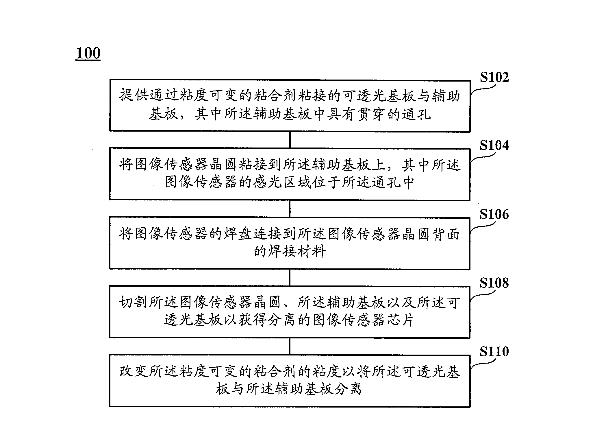
[0029] figure 1 A packaging method 100 for an image sensor according to an embodiment of the present invention is shown.

[0030] Such as figure 1 As shown, the packaging method 100 includes:

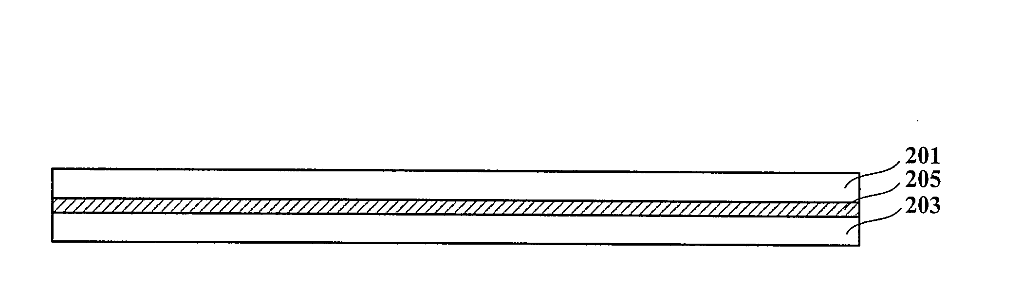
[0031] Executing step S102, providing a light-permeable substrate and an auxiliary substrate bonded by an adhesive with variable viscosity, wherein the auxiliary substrate has a through hole;

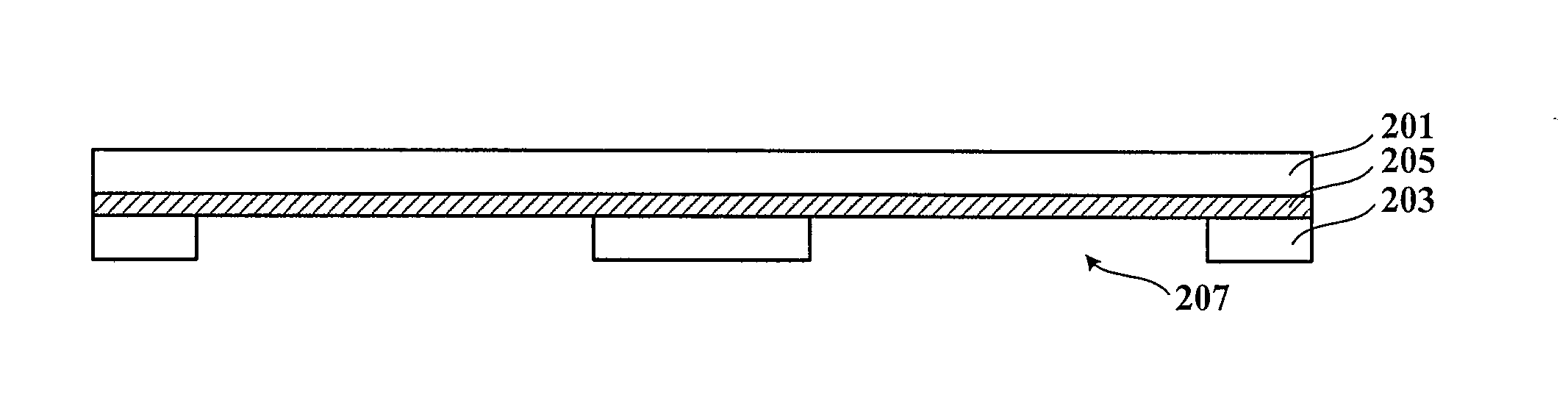
[0032] Execute step S104, bonding the image sensor wafer to the auxiliary substrate, wherein the photosensitive area of ​​the image sensor is located in the through hole;

[0033] Execute step S106, connecting the welding pad of the image sensor to the welding material on the backside of the image sensor wafer;

[0034] Execu...


PUM


Abstract

The invention discloses an image sensor packaging method, which includes: a, providing a light-transmittable substrate and an auxiliary substrate which are adhered by adhesives variable in viscosity, wherein the auxiliary substrate is internally provided with perforated through holes; b, adhering wafers of an image sensor onto the auxiliary substrate, wherein photosensitive areas of the image sensor are positioned in the through holes; c, connecting pads of the image sensor onto welding materials on the backs of the wafers; d, cutting the wafers of the image sensor, the auxiliary substrate and the light-transmittable substrate so as to obtain isolated image sensor chips; and e, changing the viscosity of the adhesives variable in viscosity so as to isolate the light-transmittable substrate from the auxiliary substrate.

Description

technical field [0001] The present invention relates to the field of semiconductor technology, and more specifically, the present invention relates to a packaging method of an image sensor. Background technique [0002] With the development of semiconductor technology, image sensors have been widely used in various fields requiring digital imaging, such as digital cameras, digital video cameras and other electronic products. According to different photoelectric conversion methods, image sensors can generally be divided into two categories: charge coupled device (Charge Coupled Device, CCD) image sensors and complementary metal oxide semiconductor (CMOS) image sensors. Among them, the CMOS image sensor has the advantages of small size, low power consumption, and low production cost. Therefore, the CMOS image sensor is easy to be integrated in portable electronic devices such as mobile phones, notebook computers, and tablet computers, as a camera module that provides digital i...

Claims


Application Information

Patent Timeline
Patent Type & Authority Applications(China)
IPC IPC(8): H01L27/146
Inventor 邓辉霍介光赵立新
Owner GALAXYCORE SHANGHAI
Why Eureka
Try Eureka