Circuit of gate drive on array, shift register and display screen

A gate integrated drive and circuit technology, used in static memory, digital memory information, instruments, etc., to ensure reliability and stability, and ensure stability.

Active Publication Date: 2012-08-08
BEIJING BOE OPTOELECTRONCIS TECH CO LTD
View PDF6 Cites 87 Cited by
  • Summary
  • Abstract
  • Description
  • Claims
  • Application Information

AI Technical Summary

Problems solved by technology

When using such a panel with the system side, due to the differences in the ICs of different system sides (IC up or down), sometimes it is necessary to reverse the image through debugging software, causing a lot of inconvenience

Method used


Image

  • Circuit of gate drive on array, shift register and display screen
  • Circuit of gate drive on array, shift register and display screen
  • Circuit of gate drive on array, shift register and display screen

Examples


Embodiment Construction

[0026] The embodiments of the present invention will be described in further detail below with reference to the accompanying drawings.

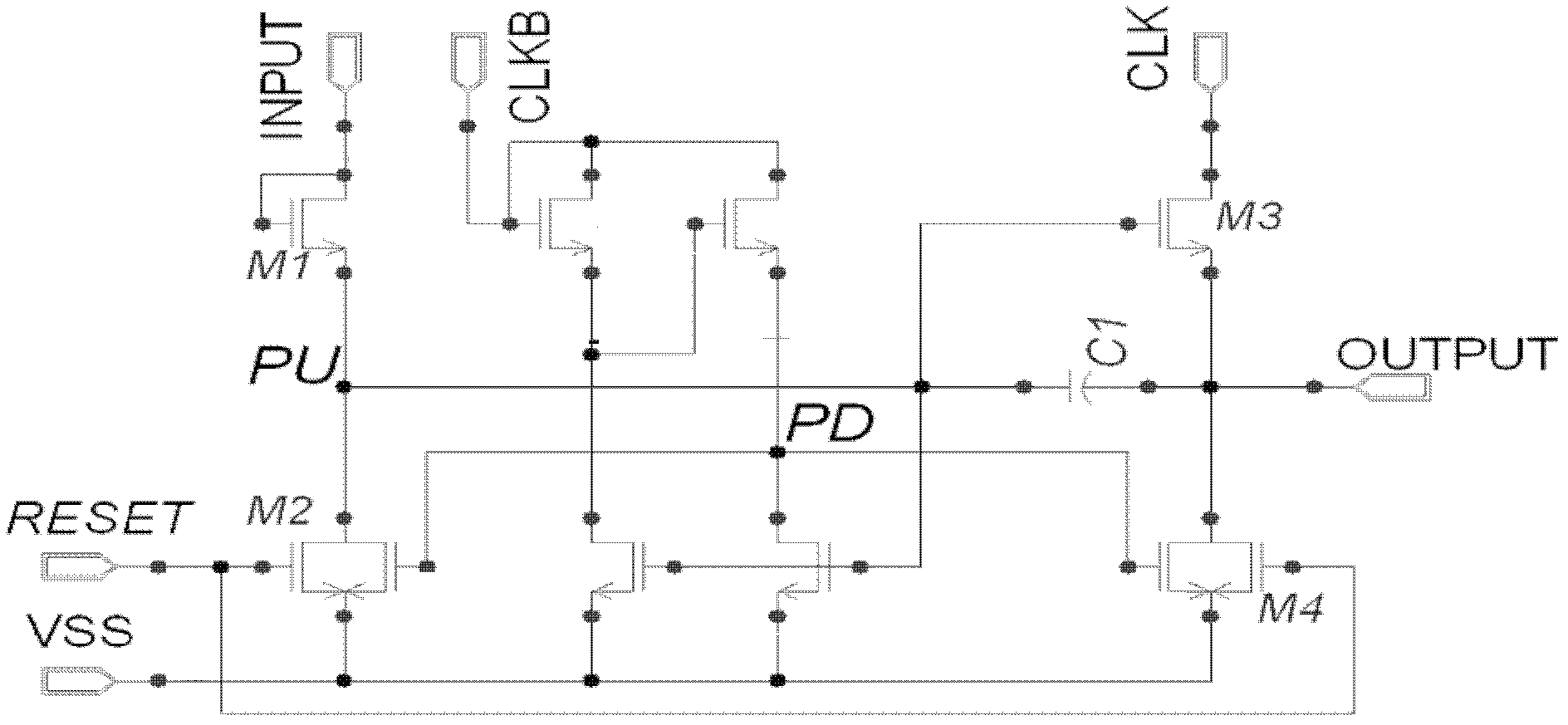
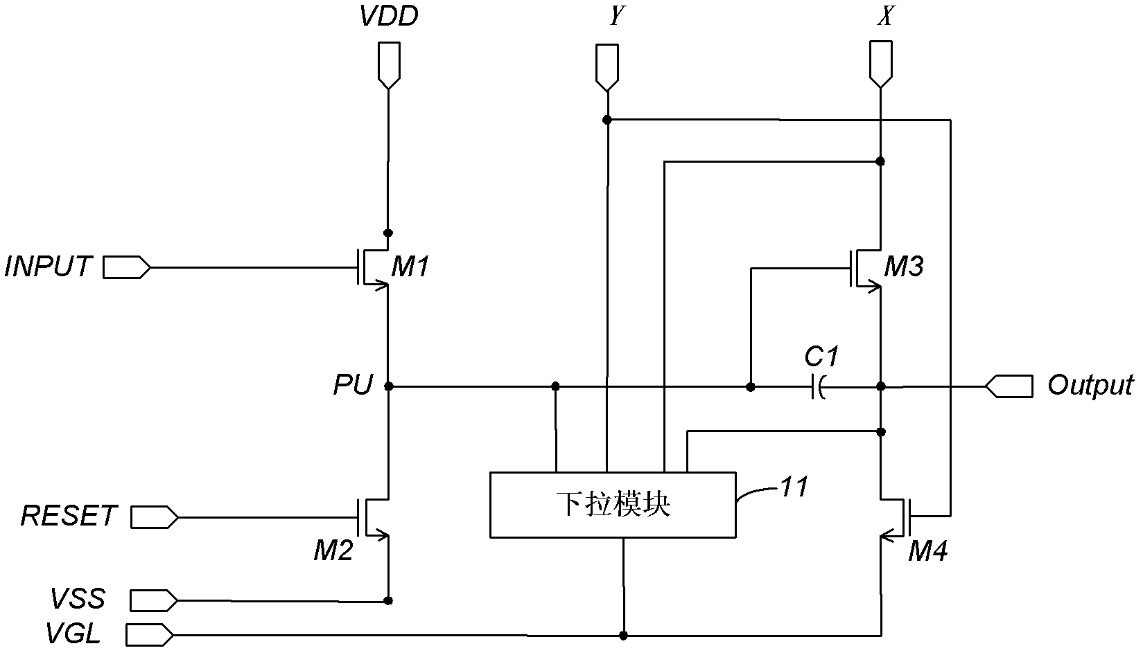
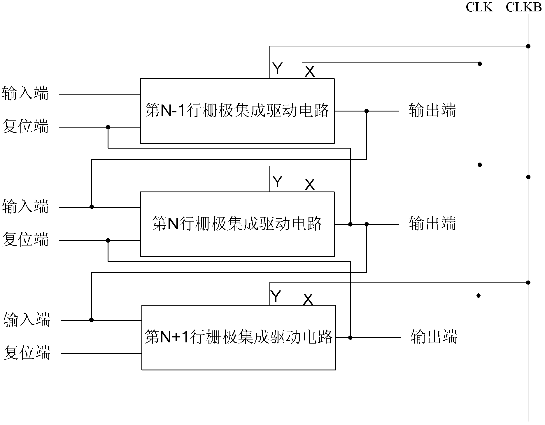
[0027] Embodiments of the present invention provide a multi-row gate integrated driving circuit, such as figure 2 As shown, the gate integrated drive circuit of this row includes:

[0028] the first thin film field effect transistor TFT M1, the gate of which is connected to the input terminal INPUT of the gate integrated driving circuit of the row, the drain is connected to the power supply voltage VDD, and the source is connected to the first node PU serving as a pull-up node;

[0029] The second TFT M2, the gate of which is connected to the reset terminal RESET of the gate integrated driving circuit of the row, the source is connected to the common connection voltage VSS, and the drain is connected to the first node PU;

[0030] The third TFT M3, the gate of which is connected to the first node PU, the drain is connected to the first cloc...


PUM


Abstract

The embodiment of the invention relates to the liquid crystal display technology field, especially to a circuit of gate drive on array (GOA), a shift register and a display screen. The GOA circuit comprises a first thin film transistor (TFT), a second TFT, a third TFT, a fourth TFT, a capacitor and a drop-down module. The drop-down module, which is connected between a first clock signal input terminal, a second clock signal input terminal, a first node and an output terminal and is connected with a low level signal terminal, is used for maintaining the first node and the output terminal to be at a low level within non-working time of the GOA circuit of this row. According to the invention, functions of an input terminal and a reset terminal in the GOA circuit are designed to be symmetrical, so that the GOA circuit can realize bilateral scanning without changing charging and discharging characteristics of a node; and thus reliability and stability of the circuit are ensured.

Description

technical field [0001] The invention relates to the technical field of liquid crystal display, in particular to a gate integrated driving circuit, a shift register and a display screen. Background technique [0002] GOA (Gate Drive on Array, gate integrated drive) refers to integrating the gate drive of an LCD (Liquid Crystal Display, liquid crystal display) panel on a glass substrate. Then the GOA circuit is connected to the gate lines of the array substrate, and acts as a shift register to control the gate line signals. Compared with the traditional COF (Chip On Film, chip on film) and COG (Chip On Glass, directly bonded glass) processes, GOA technology not only saves costs. [0003] However, in the prior art, the scanning direction of the GOA panel can only be a single direction, such as scanning from top to bottom or scanning from bottom to top, such as figure 1 As shown, it is a GOA circuit for unidirectional scanning in the prior art, and its working principle is: wh...

Claims


Application Information

Patent Timeline
Patent Type & Authority Applications(China)
IPC IPC(8): G09G3/20G09G3/36
CPCG09G3/3674G11C19/28H03K5/153G09G2310/0286G09G2310/08G09G2310/0283G09G2300/0408G09G3/20G09G3/36
Inventor 陈希
Owner BEIJING BOE OPTOELECTRONCIS TECH CO LTD
Why Eureka
Try Eureka