TFT array substrate and manufacturing method thereof and display device

A technology of an array substrate and a manufacturing method, which is applied in the fields of a TFT array substrate and a manufacturing method thereof and a display device, can solve the problems of complicated process flow, increase in thickness of the substrate, etc., and achieve the effects of simplifying the process flow, changing the thickness, and thinning the thickness.

Inactive Publication Date: 2012-08-08
BOE TECH GRP CO LTD
View PDF5 Cites 40 Cited by
  • Summary
  • Abstract
  • Description
  • Claims
  • Application Information

AI Technical Summary

Problems solved by technology

[0004] In the preparation process of the TFT array substrate in ADS mode, the preparation of the pixel electrode layer, source electrode, drain e

Method used


Image

  • TFT array substrate and manufacturing method thereof and display device
  • TFT array substrate and manufacturing method thereof and display device
  • TFT array substrate and manufacturing method thereof and display device

Examples


Embodiment Construction

[0034] The following will clearly and completely describe the technical solutions in the embodiments of the present invention with reference to the accompanying drawings in the embodiments of the present invention. Obviously, the described embodiments are only some, not all, embodiments of the present invention. Based on the embodiments of the present invention, all other embodiments obtained by persons of ordinary skill in the art without making creative efforts belong to the protection scope of the present invention.

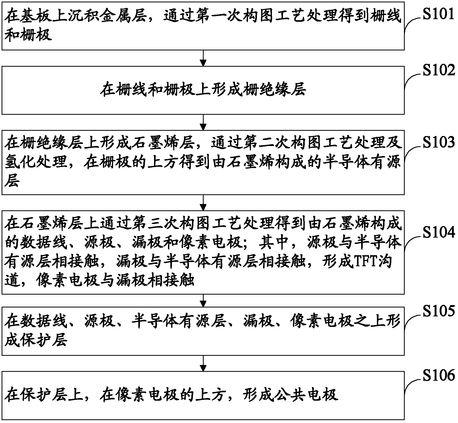
[0035] The TFT array substrate manufacturing method provided by the embodiment of the present invention, such as figure 1 As shown, the steps include:

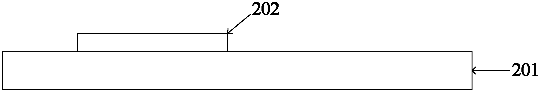
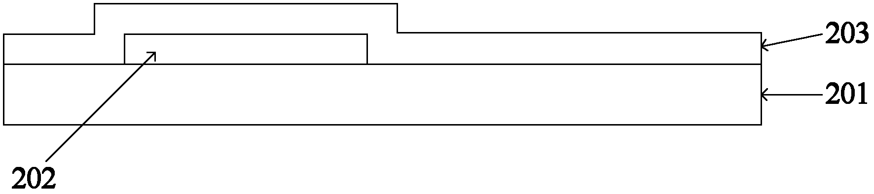
[0036] S101 , depositing a metal layer on the substrate, and obtaining gate lines and gates through a first patterning process.

[0037] Such as figure 2 As shown, a magnetron sputtering method can be used to prepare a layer with a thickness of to metal film layer. The metal material can usually be met...


PUM


Abstract

The invention, which relates to the display technology field, provides a thin film transistor (TFT) array substrate and a manufacturing method thereof and a display device, so that a TFT array substrate structure in an advanced super dimension switch (ADS) mode is improved to thin the thickness of the substrate and the process flow is also simplified. The TFT array substrate manufacturing method comprises: obtaining a gate line and a gate electrode on a glass substrate by processing with utilization of a first-time composition process; forming a gate insulation layer on the gate line and the gate electrode; forming a graphene layer on the gate insulation layer and carrying out processing with utilization of a second-time composition process and hydrotreating to obtain a semiconductor active layer above the gate electrode; carrying out processing with utilization of a third-time composition process to obtain a data line, a source electrode, a drain electrode and a pixel electrode at a same layer; forming a protective layer on the data line, the source electrode, the semiconductor active layer, the drain electrode and the pixel electrode; and forming a common electrode on the protective layer above the pixel electrode. According to the embodiment of the invention, the method is applied to manufacture a TFT array substrate in an ADS mode.

Description

technical field [0001] The invention relates to the field of display technology, in particular to a TFT array substrate, a manufacturing method thereof, and a display device. Background technique [0002] TFT-LCD (Thin Film Transistor-Liquid Crystal Display, Thin Film Field Effect Transistor Liquid Crystal Display) uses the change of the electric field intensity set on the liquid crystal layer to change the degree of rotation of liquid crystal molecules, thereby controlling the intensity of light transmission to display images . Generally speaking, a complete liquid crystal display panel must have a backlight module group, a polarizer, an upper substrate (usually a color filter substrate), a lower substrate (usually an array substrate), and a box filled with the two substrates. Layers of liquid crystal molecules. On the array substrate, data lines and gate lines intersecting horizontally and vertically are formed, and the data lines and gate lines surround pixel units arra...

Claims


Application Information

Patent Timeline
IPC IPC(8): H01L21/77H01L27/02H01L29/786G02F1/1362G02F1/1368
CPCG02F1/1362H01L27/02H01L21/77H01L29/786G02F1/1368H01L27/124H01L29/66742H01L29/78684H10K59/1213H01L29/1606
Inventor 戴天明薛建设姚琪张锋
Owner BOE TECH GRP CO LTD
Why Eureka
Try Eureka