Thin film transistor array substrate and manufacturing method thereof

A technology of thin film transistors and array substrates, applied in the field of thin film transistor array substrates and its production, can solve the problems of low yield rate, high product cost, and excessive mask exposure times

Active Publication Date: 2012-08-08
BOE TECH GRP CO LTD
View PDF3 Cites 8 Cited by
  • Summary
  • Abstract
  • Description
  • Claims
  • Application Information

AI Technical Summary

Problems solved by technology

[0005] Embodiments of the present invention provide a thin film transistor array substrate and a manufacturing method thereof, which are used to solve the problems in the prior art, such as high product cost, low yield rate and equipment The problem of low productivity

Method used


Image

  • Thin film transistor array substrate and manufacturing method thereof
  • Thin film transistor array substrate and manufacturing method thereof
  • Thin film transistor array substrate and manufacturing method thereof

Examples


Embodiment Construction

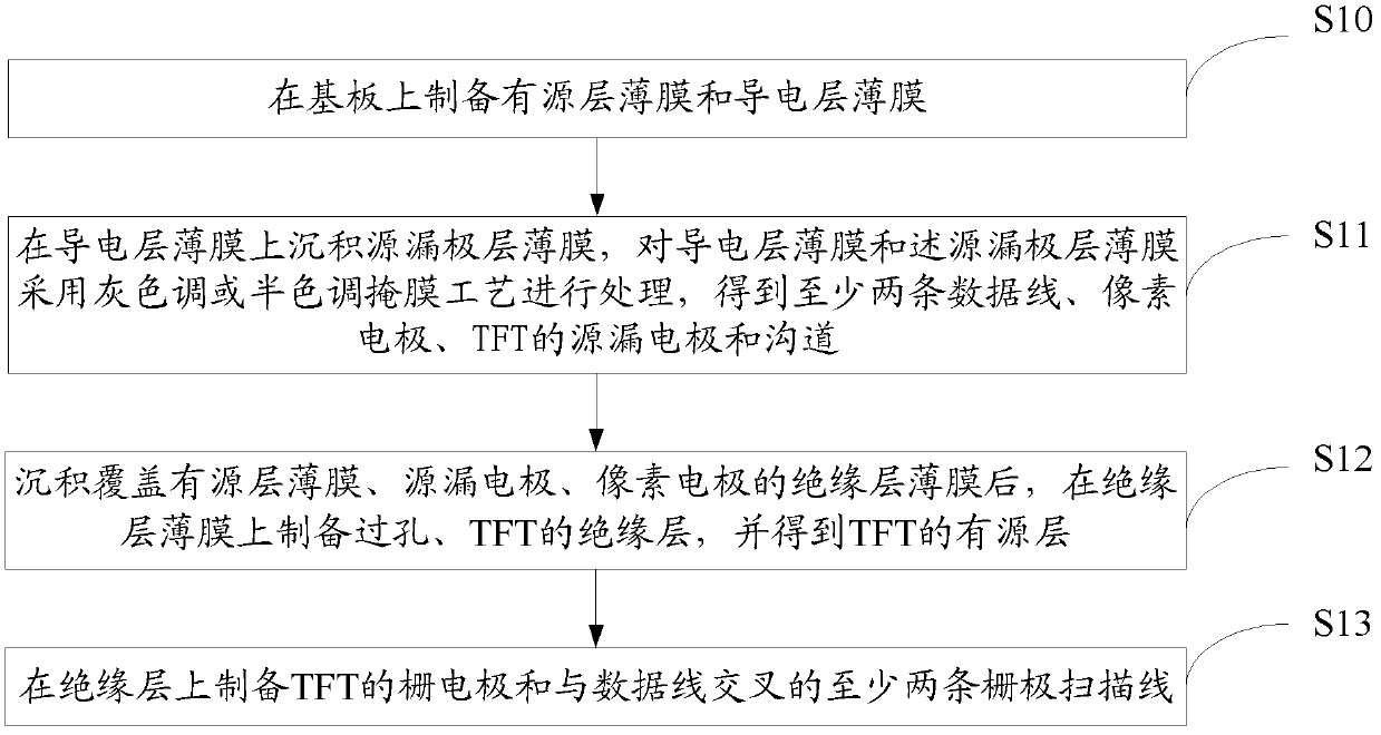
[0028] Aiming at the problems of high product cost, low yield rate and low equipment capacity caused by too many mask exposure times in the process of manufacturing a thin film transistor array substrate in the prior art, an embodiment of the present invention provides a method for manufacturing a thin film transistor array substrate method, the flow of the method is as follows figure 1 As shown, the specific execution steps are as follows:

[0029] S10: preparing an active layer thin film and a conductive layer thin film on the substrate.

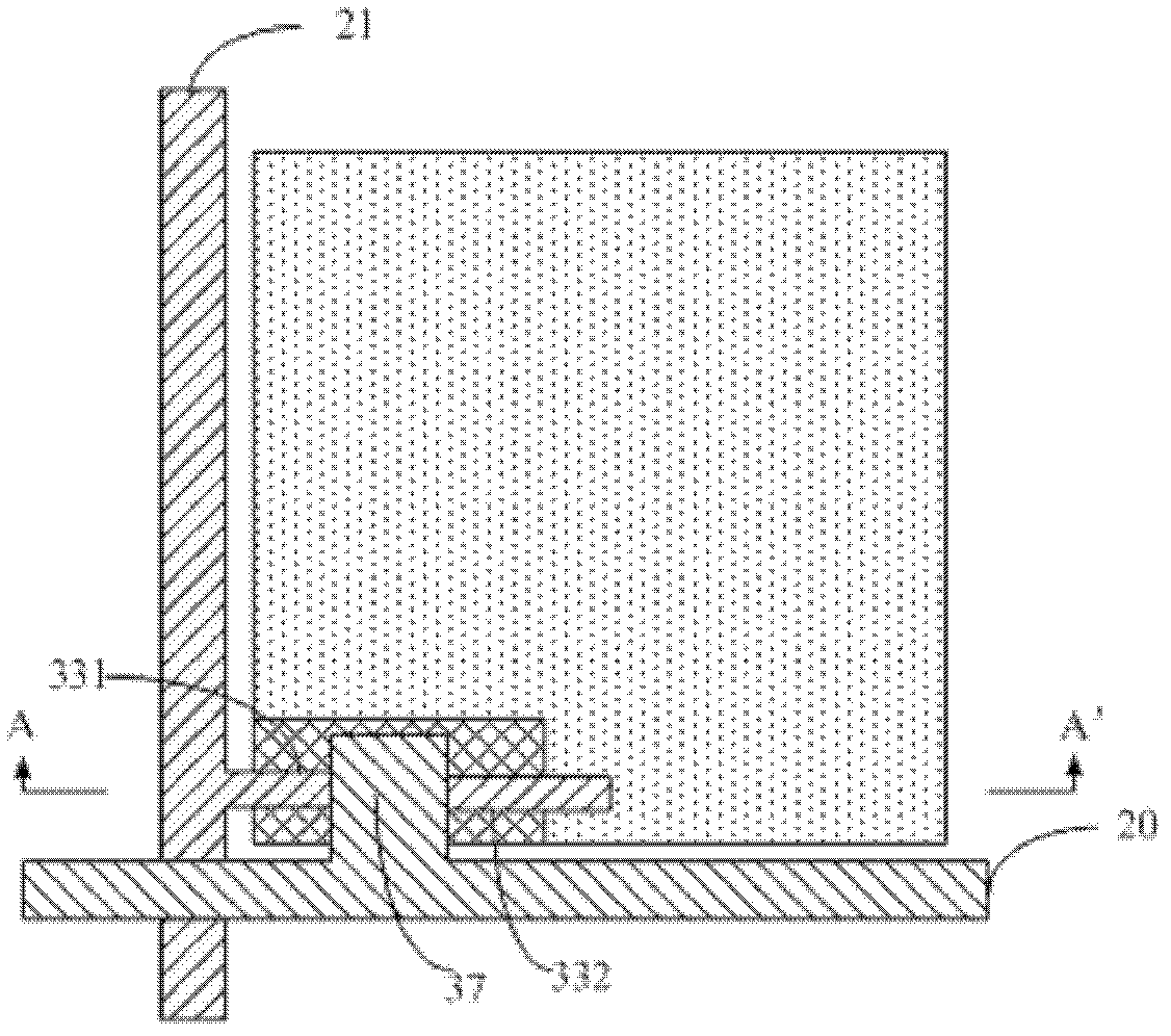
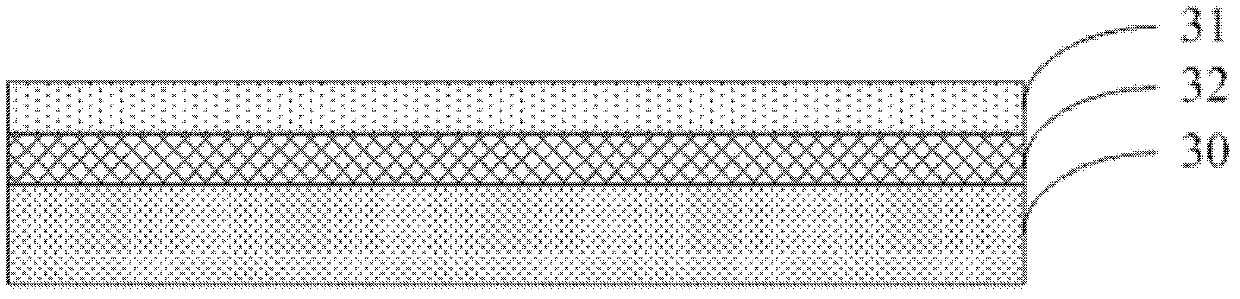
[0030] S11: Deposit the source-drain layer film on the conductive layer film, and process the conductive layer film and the source-drain layer film with a gray-tone or half-tone masking process to obtain at least two data lines, pixel electrodes, and TFT sources The drain electrode and the channel; the source of a row of TFTs on the array substrate is connected to a data line.

[0031] S12: After depositing the insulating layer film cove...


PUM

PropertyMeasurementUnit
thicknessaaaaaaaaaa
thicknessaaaaaaaaaa
thicknessaaaaaaaaaa

Abstract

The invention discloses a thin film transistor array substrate and a manufacturing method thereof. The manufacturing method comprises the following steps: preparing an active layer film and a conducting layer film on the substrate; depositing a source drain layer film on the conducting layer film, using a gray tone or halftone mask process to process the conducting layer film and the source drain layer film so as to obtain at least two data lines, a pixel electrode, a source drain electrode of the TFT (thin film transistor) and a channel; making a source electrode of one column of the TFT on the array substrate connect with one data line; after depositing an insulating layer film which covers the active layer film, the source drain electrode, the data lines and the pixel electrode, preparing via and an insulating layer of the TFT on the insulating layer film and obtaining the active layer of the TFT; preparing a gate electrode of the TFT and at least two grid scanning lines which are intersected with the data lines, and making the gate electrode of one row of the TFT on the array substrate connect with one grid scanning line. By using the method of the invention, product cost can be reduced, and a yield and an equipment capacity can be increased.

Description

technical field [0001] The invention relates to the field of display technology, in particular to a thin film transistor array substrate and a manufacturing method thereof. Background technique [0002] Currently, flat panel displays are mostly used in the display field, and most of the flat panel display devices are active matrix liquid crystal display devices (Active Matrix / Organic Liquid Crystal Display, AMLCD). Existing AMLCD devices include thin film transistor (Thin Film Transistor, TFT) array substrates. Since amorphous silicon a-Si is easy to realize large-area preparation at low temperature, and the preparation technology is relatively mature, it is currently the most popular method for manufacturing TFT array substrates. widely used material. However, the bandgap of the a-Si material is only 1.7V, it is opaque to visible light, and has photosensitivity in the visible light range, so it is necessary to add an opaque metal mask (black matrix) to block light, which i...

Claims


Application Information

Patent Timeline
Patent Type & Authority Applications(China)
IPC IPC(8): H01L21/77H01L27/12G02F1/1368
CPCH01L21/77H01L27/1288H01L27/1225H01L27/1259H01L27/12H01L27/124G02F1/136286H01L29/41733H01L29/78618H01L27/127
Inventor 宁策吕志军
Owner BOE TECH GRP CO LTD
Why Eureka
Try Eureka