Decomposition and marking of semiconductor device design layout in double patterning lithography

A design layout, double graphics technology, applied in the field of photomasks, can solve problems such as DPL technology troubles

Active Publication Date: 2012-08-15
TAIWAN SEMICON MFG CO LTD
View PDF6 Cites 9 Cited by
  • Summary
  • Abstract
  • Description
  • Claims
  • Application Information

AI Technical Summary

Problems solved by technology

[0005] Therefore, existing DPL techniques are plagued by various deficiencies and limitations

Method used


Image

  • Decomposition and marking of semiconductor device design layout in double patterning lithography
  • Decomposition and marking of semiconductor device design layout in double patterning lithography
  • Decomposition and marking of semiconductor device design layout in double patterning lithography

Examples


Embodiment Construction

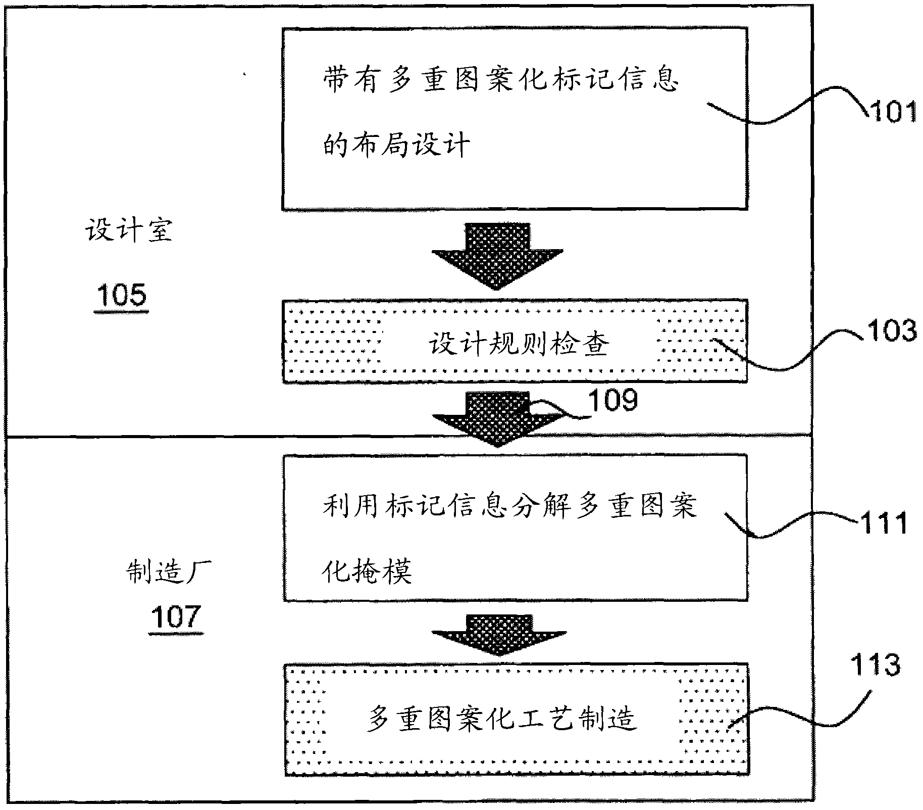
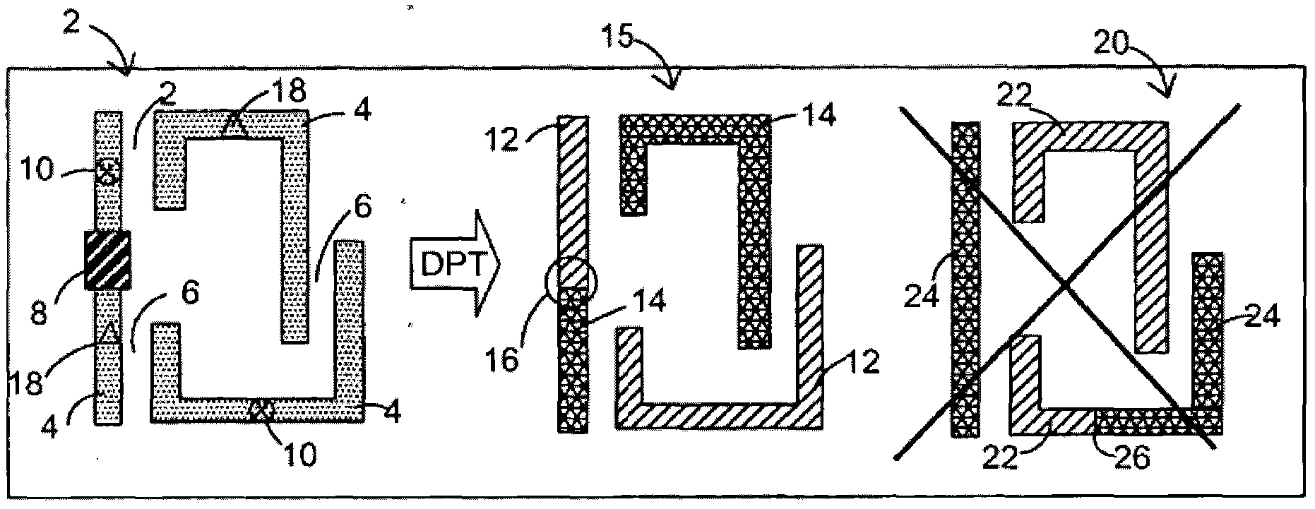
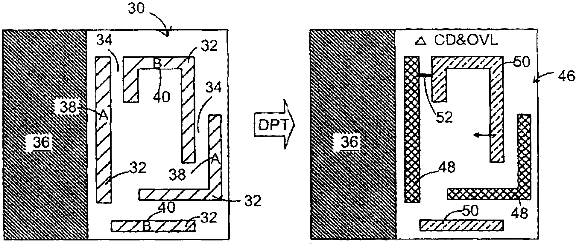
[0032] A design layout represents the exposed pattern to be formed on the semiconductor device. The design layout may be provided to the mask foundry by being stored on a computer readable electronic storage medium or other electronic file or in other suitable ways. Decompose the device components of the designed layout into two separate photomasks that are used to form specific exposure patterns. On a design level (ie, a design layout provided to a mask foundry), device components to be decomposed onto the first mask and device components to be decomposed onto the second mask are indicated. The stitching locations are also indicated on the design level (ie, the design layout provided to the mask foundry). At a stitching location, features from two different decomposed masks are stitched together to form a continuous feature. The design layout provided to the mask foundry contains markings associating components with either the first photomask or the second photomask and the...


PUM


Abstract

Provided is a system and method for assessing a design layout for a semiconductor device level and for determining and designating different features of the design layout to be formed by different photomasks by decomposing the design layout. The features are designated by markings that associate the various device features with the multiple photomasks upon which they will be formed and then produced on a semiconductor device level using double patterning lithography, DPL, techniques. The markings are done at the device level and are included on the electronic file provided by the design house to the photomask foundry. In addition to overlay and critical dimension considerations for the design layout being decomposed, various other device criteria, design criteria processing criteria and their interrelation are taken into account, as well as device environment and the other device layers, when determining and marking the various device features.

Description

technical field [0001] The present invention generally relates to photomasks for use in the manufacture of semiconductor devices, and to the manufacture of such photomasks. More specifically, the present invention relates to Double Patterning Lithography (DPL) device layout decomposition for photomasks. Background technique [0002] In today's semiconductor manufacturing industry, large scale integration (LSI) devices continue to evolve in increasing levels of integration and complexity. These increased levels of integration require the improvement and manufacture of sophisticated and highly accurate LSI patterns. These patterns require highly accurate patterning techniques to form precise pattern parts. According to conventional techniques, a semiconductor device such as an integrated circuit is formed on a semiconductor substrate using an arrangement of photomasks, each of which is used to form a complete exposure pattern of a specific device level. The exposed pattern,...

Claims


Application Information

Patent Timeline
Patent Type & Authority Applications(China)
IPC IPC(8): G03F7/14H01L27/02
CPCG03F1/70G03F7/70433G03F7/70466
Inventor 徐金厂杨稳儒赵孝蜀郑仪侃鲁立忠
Owner TAIWAN SEMICON MFG CO LTD
Why Eureka
Try Eureka