PCB (printed circuit board) packaging architecture method

A packaging library and mounting hole technology, applied in special data processing applications, instruments, electrical digital data processing, etc., can solve the problems of prolonging the design cycle, increasing the design workload, increasing the complexity of PCB design and error rework rate, etc., to achieve Reduce duplication of work, facilitate layout and wiring design, reduce the effect of error rate and rework rate

Inactive Publication Date: 2012-08-15
NAT UNIV OF DEFENSE TECH
View PDF4 Cites 13 Cited by
  • Summary
  • Abstract
  • Description
  • Claims
  • Application Information

AI Technical Summary

Problems solved by technology

[0004] The traditional method mentioned above greatly increases the complexity and error rework ra

Method used


Image

  • PCB (printed circuit board) packaging architecture method
  • PCB (printed circuit board) packaging architecture method
  • PCB (printed circuit board) packaging architecture method

Examples


Example Embodiment

[0036] Example 1 :

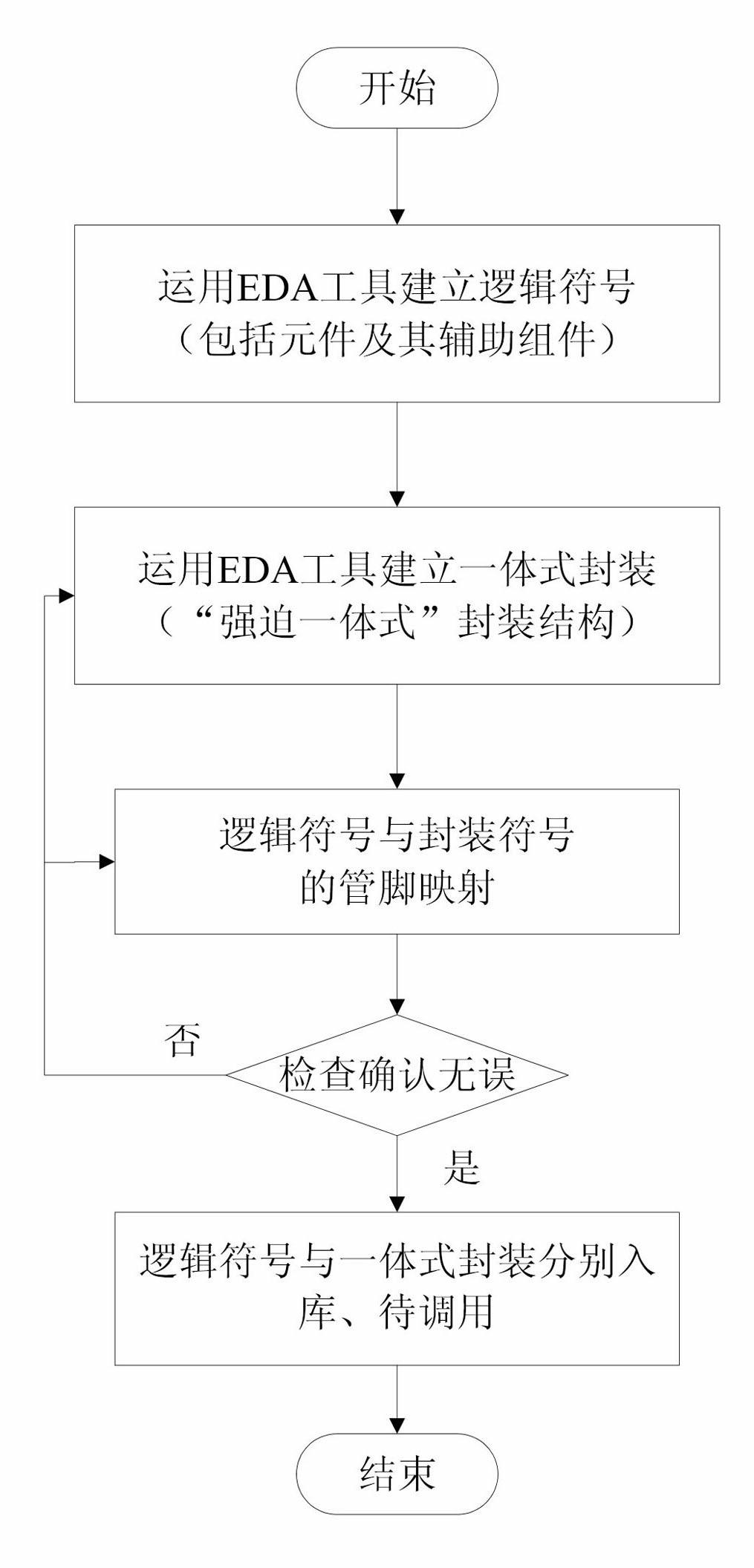
[0037] Such as figure 1 As shown, the PCB packaging structure method of this embodiment includes the following steps:
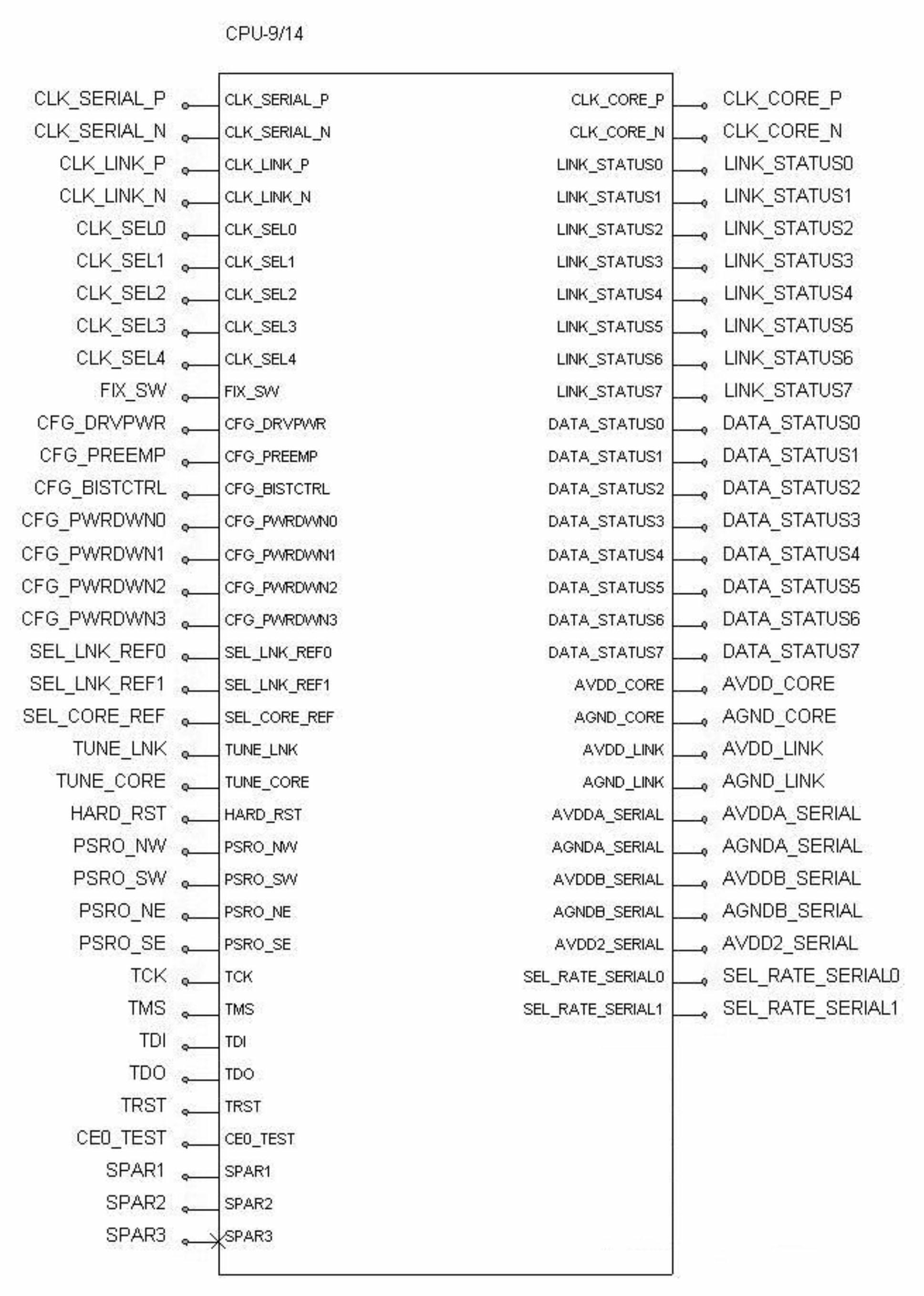
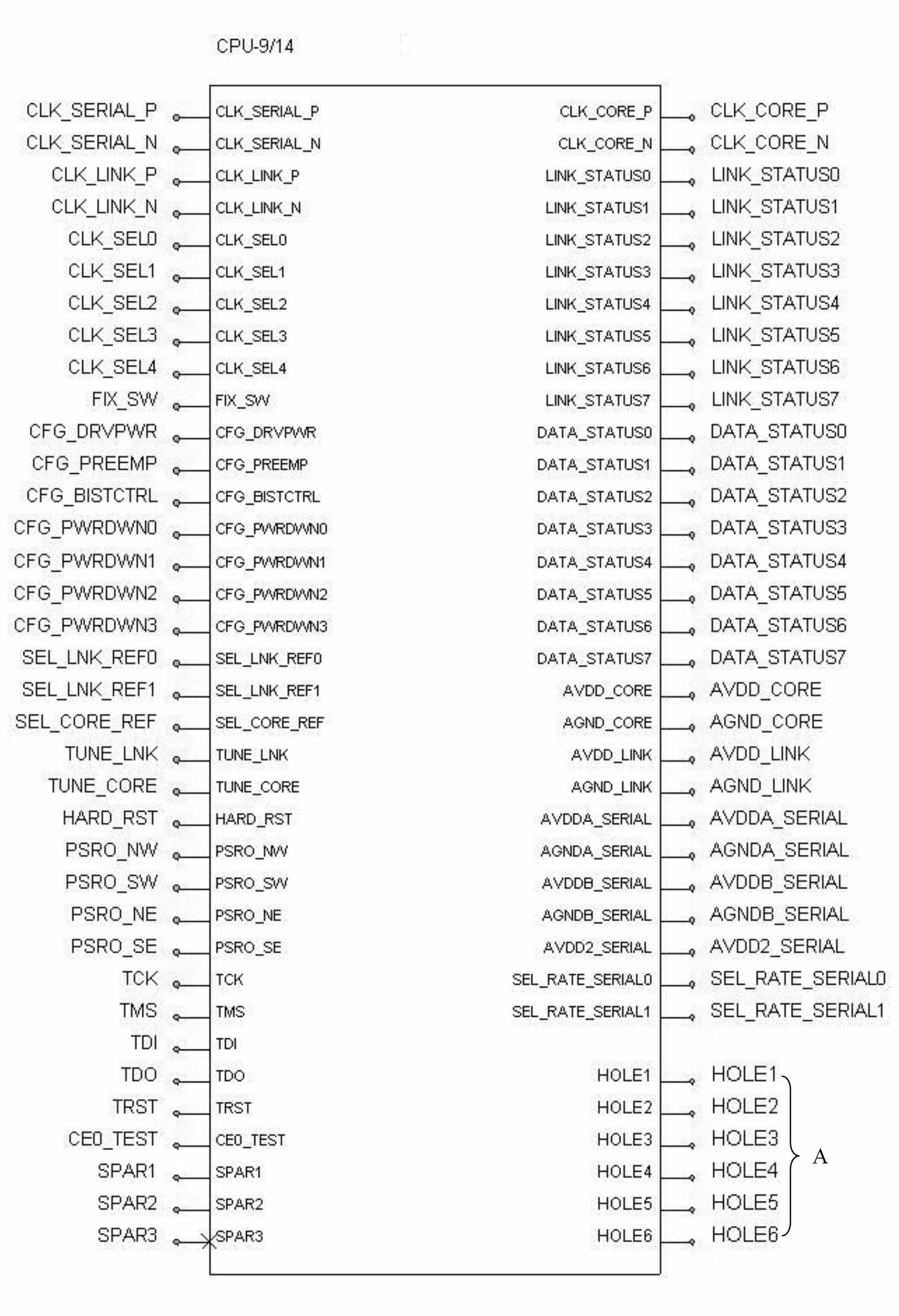
[0038] 1. Such as image 3 As shown, a logic symbol is established in the logic symbol library, and the logic symbol includes pins and mounting holes of components and auxiliary components. Among them, the auxiliary components of the component include: heat dissipation components, positioning components and structural firmware. The aforementioned logical symbols (see image 3 ) Is like figure 2 The traditional logic symbols of the components are made by adding auxiliary component pins and mounting holes logic, image 3 Middle A is the logic of mounting holes and positioning holes required for structure and heat dissipation.

[0039] 2. Establish traditional package symbols for components (such as Figure 4 As shown), an auxiliary package symbol is established according to the structural characteristics of the auxiliary component of the compon...

Example Embodiment

[0043] Example 2:

[0044] Such as Image 6 As shown, the PCB packaging structure method of the present invention includes the following steps:

[0045] 1. Create a traditional logic symbol of a component in the logic symbol library (such as Figure 7 Shown); create a new auxiliary logic symbol (such as Figure 8 As shown), the auxiliary logic symbol includes the logic of the pin and mounting hole of the auxiliary component of the component, and the traditional logic symbol is automatically associated with the auxiliary logic symbol. Among them, the auxiliary components of the component include: heat dissipation components, positioning components, and structural firmware.

[0046] 2. Establish traditional package symbols for components (such as Picture 9 Shown), and then create an auxiliary package symbol according to the structural characteristics of the auxiliary component of the component (such as Picture 10 As shown), the auxiliary package symbol includes the package of the p...


PUM


Abstract

The invention discloses a PCB (printed circuit board) packaging architecture method, which includes the steps: setting up a logic symbol in a logic symbol library, wherein the logic symbol comprises pins and mounting holes of an element and an auxiliary component thereof; setting up a traditional packaging symbol of the element, setting up an auxiliary packaging symbol according to the structural characteristics of the auxiliary component of the element, and combining the traditional packaging symbol and the auxiliary packaging symbol into integrated package or associating the traditional packaging symbol with the auxiliary packaging symbol into a combined packaging symbol; and mapping the logic symbol and the corresponding integrated package or combined package, and storing the integrated package or combined package into a PCB packaging bank for integral calling or combination calling. Using the PCB packaging architecture method can improve operating efficiency, reduce repetitive operations in PCB design and improve PCB design accuracy.

Description

technical field [0001] The invention relates to PCB (printed board) design, in particular to a method for PCB package structure. Background technique [0002] Integrated circuit packaging not only plays the role of connecting the bonding points in the integrated circuit chip with the external circuit, but also provides a stable and reliable working environment for the integrated circuit chip, and protects the integrated circuit chip mechanically or environmentally, so that the integrated circuit The chip can perform normal functions, and its high stability and reliability are guaranteed. With the continuous development of wafer technology, the size of transistors continues to decrease. According to Moore's Law, the number of transistors that can be accommodated on an integrated circuit will double every 18 months, and the performance will also double; Therefore, the complexity of integrated circuit packaging is also constantly increasing, and the packaging form has also dev...

Claims


Application Information

Patent Timeline
IPC IPC(8): G06F17/50
Inventor 曹跃胜陈超肖立权李晋文胡军陈旭罗煜峰蒋句平李元山田宝华宋飞
Owner NAT UNIV OF DEFENSE TECH
Why Eureka
Try Eureka