Drive circuit structure of spatial light modulator

A technology of spatial light modulator and driving circuit, applied in instruments, static indicators, etc., can solve the problems of multi-chip area, limitation, occupation, etc., and achieve the effect of reducing chip area, increasing transmission bandwidth, and increasing data transmission rate

Inactive Publication Date: 2012-08-22
SUZHOU INST OF NANO TECH & NANO BIONICS CHINESE ACEDEMY OF SCI
View PDF7 Cites 2 Cited by
  • Summary
  • Abstract
  • Description
  • Claims
  • Application Information

AI Technical Summary

Problems solved by technology

There are two main disadvantages of this design: 1. The DAC array is at the same level as the pixel array, which occupies a lot of chip area; 2. The data input rate and the number of DACs limit faster and more electro-optical signal conversion.

Method used


Image

  • Drive circuit structure of spatial light modulator
  • Drive circuit structure of spatial light modulator
  • Drive circuit structure of spatial light modulator

Examples


Embodiment Construction

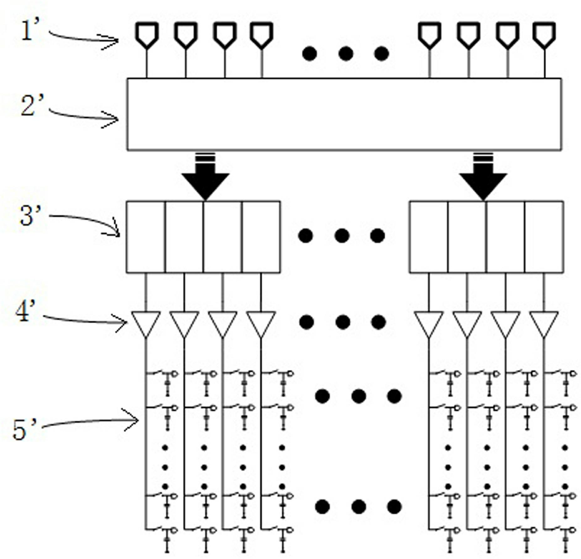
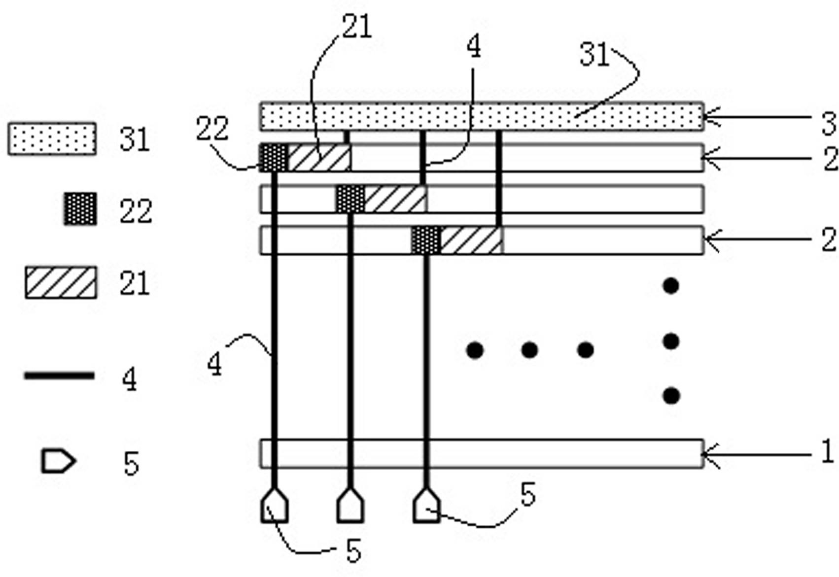
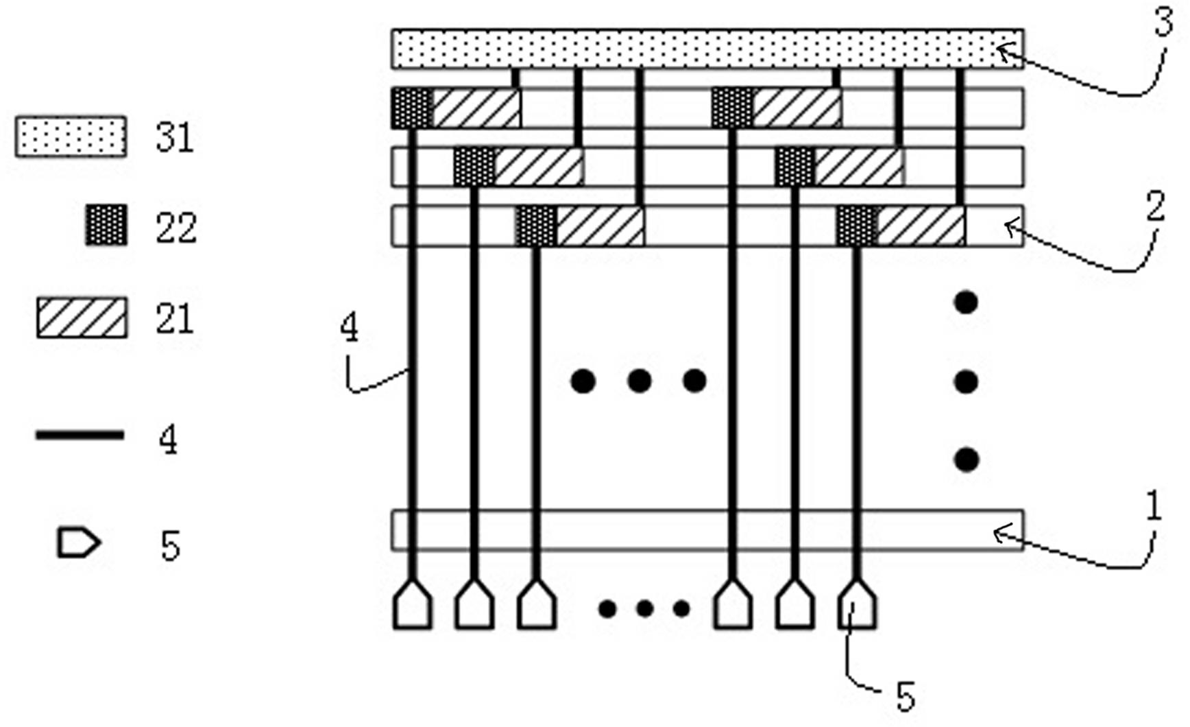
[0019] like figure 2 As shown in the figure, the drive circuit structure of the spatial light modulator in this embodiment includes a chip selection chip 1, a plurality of data register and digital-to-analog conversion chips 2 and a drive chip 3, which are arranged in sequence from bottom to top. The vertical direction is stacked layer by layer.

[0020] A pixel unit array 31 is integrated in the driving chip 3 . A plurality of digital-to-analog converters 21 distributed at intervals are integrated in the data storage and digital-to-analog replacement chip 2 (these digital-to-analog converters distributed at intervals constitute a digital-to-analog converter array), and each digital-to-analog converter 21 is adjacent to the Each is arranged with a data storage unit 22 immediately adjacent thereto. Each digital-to-analog converter 21 and the driver chip 3 are electrically connected through through silicon vias 4; and each data storage unit 22 and the chip selection chip 1 ar...


PUM


Abstract

The invention discloses a drive circuit structure of a spatial light modulator, which comprises a chip selection chip, a plurality of data register and digital-to-analogue conversion chips, and a drive chip, wherein a plurality of digital-to-analogue converters arranged at intervals are integrated in the data register and digital-to-analogue conversion chips, a data storage unit adjacent to each digital-to-analogue converter is arranged near the digital-to-analogue converter, and each digital-to-analogue converter is electrically connected with the drive chip through a through-silicon opening and each data storage unit is electrically connected with the chip selection chip through a through-silicon opening. The drive circuit structure has higher integrity and can support transmission of a plurality of high-speed signals.

Description

technical field [0001] The invention relates to a drive circuit structure of a spatial light modulator. Background technique [0002] The combination of CMOS driver circuit and spatial light modulator to realize photoelectric signal conversion has been applied in many occasions such as image recognition, signal processing, optical communication and optical computing. The response speed of the spatial light modulator based on the multi-quantum well process is about 1ns, which has a unique advantage in high-speed computing, and the computational complexity will not increase with the increase of device pixels, and the larger the computing advantage, the more obvious. However, traditional CMOS driver circuits cannot cooperate with modulators for high-speed optical computing. Taking a spatial light modulator array with 256*256 pixels and 256-level (8-bit) modulation grayscale as an example, the required data amount is 524,288 (256*256*8) bits / frame. To achieve high-speed optica...

Claims


Application Information

Patent Timeline
Patent Type & Authority Applications(China)
IPC IPC(8): G09G3/20G09G3/36
Inventor 朱明皓张宇翔张耀辉
Owner SUZHOU INST OF NANO TECH & NANO BIONICS CHINESE ACEDEMY OF SCI
Why Eureka
Try Eureka