Back electrode structure of back contact silicon solar cell panel and manufacture method thereof

A technology of silicon solar cells and back electrodes, applied in the field of solar cells, can solve the problems of high cost, cumbersome operation, and high price of conductive adhesive, and achieve the effects of low cost, simple preparation method, increased reliability and service life

Active Publication Date: 2012-08-22
CSI CELLS CO LTD +1
View PDF7 Cites 23 Cited by
  • Summary
  • Abstract
  • Description
  • Claims
  • Application Information

AI Technical Summary

Problems solved by technology

However, insulating gaskets need to be cut and punched, and the operations in the production of corresponding components are also relatively cumbersome
The price of the conductive backplane and the conductive glue needed to use the conductive backplane are relatively high, and the cost is relatively high.

Method used


Image

  • Back electrode structure of back contact silicon solar cell panel and manufacture method thereof
  • Back electrode structure of back contact silicon solar cell panel and manufacture method thereof
  • Back electrode structure of back contact silicon solar cell panel and manufacture method thereof

Examples


Embodiment 1

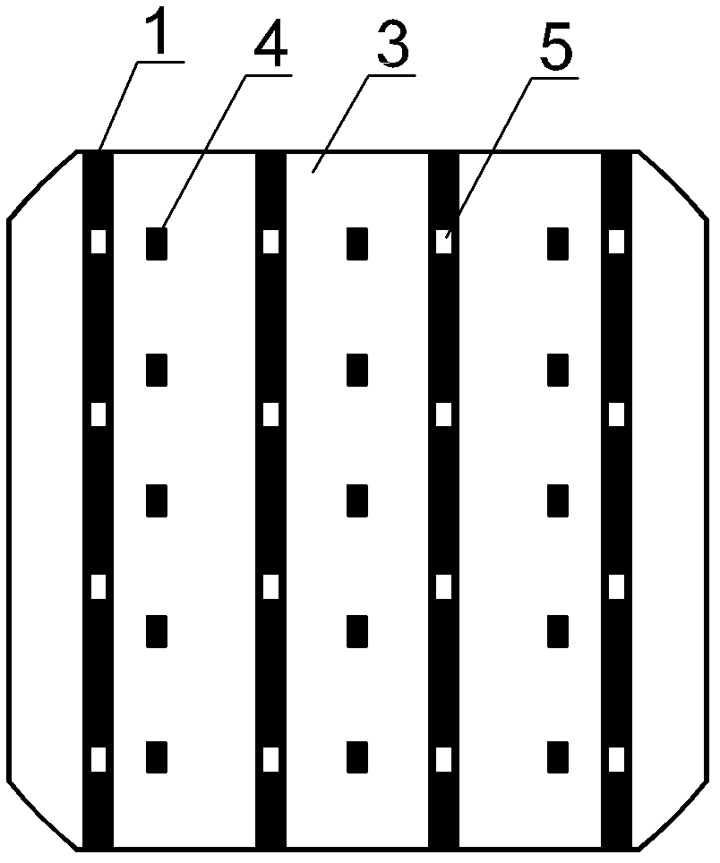
[0041] see figure 1 , 4 , shown in 5, a back electrode structure of a back contact silicon solar cell, the back side of the cell 3 is provided with a positive pole 4, a negative pole 5 and a back electric field; the polarity of the positive pole and the back electric field is the same; the negative pole Arranged side by side to form 4 negative electrode columns; the surface of each negative electrode column is covered with a strip-shaped insulating film layer 1, the number of insulating film layers is the same as the number of negative electrode columns, and the insulating film layer Extending along its length to both ends of the battery sheet;

[0042] Electrode windows are opened on the insulating adhesive film layer relative to the positions of the negative electrodes.

[0043] The insulating film layer has a thickness of 25-30 microns and a width of 5 mm. The insulating adhesive film layer is a polyester insulating adhesive film layer. The electrode window is rectangul...

Embodiment 2

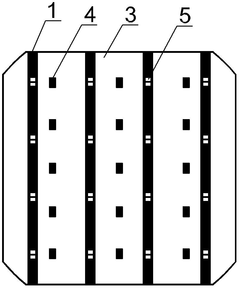
[0050] see figure 2 As shown, a back electrode structure of a back contact silicon solar cell, the back of the cell 3 is provided with a positive pole 4, a negative pole 5 and a back electric field; the polarity of the positive pole and the back electric field is the same; the negative poles are arranged side by side , forming 4 rows of negative electrode columns; the surface of each negative electrode column is covered with a strip-shaped insulating film layer 1, the number of insulating film layers is the same as the number of negative electrode columns, and the insulating film layer is along its The length direction extends to both ends of the battery sheet;

[0051] Electrode windows are opened on the insulating adhesive film layer relative to the positions of the negative electrodes.

[0052] The insulating film layer has a thickness of 20 microns and a width of 6 mm. The insulating adhesive film layer is a polyester insulating adhesive film layer. The electrode windo...

Embodiment 3

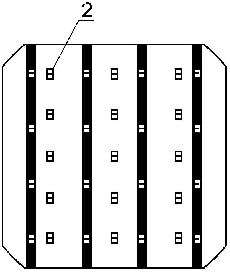
[0054] see image 3 As shown, a back electrode structure of a back contact silicon solar cell, the back of the cell is provided with a positive pole, a negative pole and a back electric field; the polarity of the positive pole and the back electric field is the same; the negative poles are arranged side by side to form 4 Negative electrode column; the surface of each negative electrode column is covered with a strip-shaped insulating adhesive film layer, the number of insulating adhesive film layers is the same as the number of negative electrode columns, and the insulating adhesive film layer extends along its length to Both ends of the cell;

[0055] Electrode windows are opened on the insulating adhesive film layer relative to the positions of the negative electrodes.

[0056] The thickness of the insulating adhesive film layer is 40 microns. The insulating adhesive film layer is a polyester insulating adhesive film layer. The electrode window is in the shape of a sun. ...


PUM


Abstract

The invention discloses a back electrode structure of a back contact silicon solar cell panel. The back of a cell panel is provided with a first electrode, second electrodes and a back electric field. Polarity of the first electrode and the second electrodes is different, and the polarity of the first electrode and the back electric field is the same. The second electrodes are arranged in parallel to form at least two second electrode lines. Strip-shaped insulation rubber film layers are covered on the surfaces of areas where the second electrode lines are located, the number of the insulation rubber film layers is the same as the line quantity of the second electrode lines, and at least one ends of the insulation rubber film layers extend to the end of the cell panel along the length direction. Electrode windows are arranged at positions on the insulation rubber film layers corresponding to the second electrodes. By means of a method of arranging the insulation rubber film layers at positions of the electrodes of the back contact silicon solar cell panel, insulation of positive electrodes and negative electrodes is achieved. The back electrode structure can well meet insulation requirements, connection between the cell panels is facilitated, and production efficiency of back contact cell assembly manufacture is greatly improved.

Description

technical field [0001] The invention relates to a back electrode structure of a back contact silicon solar cell and a preparation method thereof, belonging to the field of solar cells. Background technique [0002] Conventional fossil fuels are being exhausted day by day. Among the existing sustainable energy sources, solar energy is undoubtedly the cleanest, most common and most potential alternative energy source. At present, among all solar cells, crystalline silicon solar cells are one of the solar cells that have been widely commercialized. This is due to the extremely abundant reserves of silicon materials in the earth's crust. , has excellent electrical and mechanical properties. Therefore, crystalline silicon solar cells occupy an important position in the field of photovoltaics. High efficiency is the current development trend of crystalline silicon solar cells. The conversion efficiency of solar cells is improved by improving surface texture, selective emission j...

Claims


Application Information

Patent Timeline
Patent Type & Authority Applications(China)
IPC IPC(8): H01L31/0224H01L31/18
CPCY02P70/50
Inventor 刘宝信沈坚王栩生章灵军
Owner CSI CELLS CO LTD
Why Eureka
Try Eureka