

Resin composition for optical semiconductor element housing package, and optical semiconductor light-emitting device obtained using the same
A technology of optical semiconductor and resin composition, which is applied in the direction of semiconductor devices, electrical components, electric solid devices, etc., to achieve the effects of excellent solder heat resistance, reduced linear expansion coefficient, and good light reflectivity
- Summary
- Abstract
- Description
- Claims
- Application Information
AI Technical Summary
Problems solved by technology
Method used
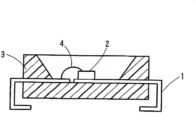
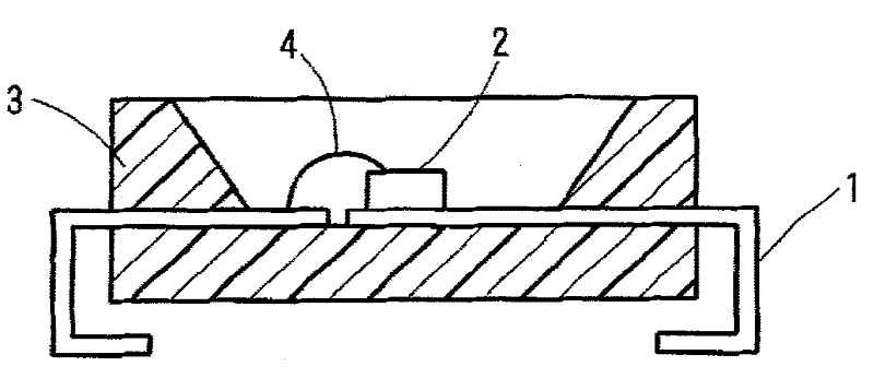
Image

Examples
Embodiment 1 to 6
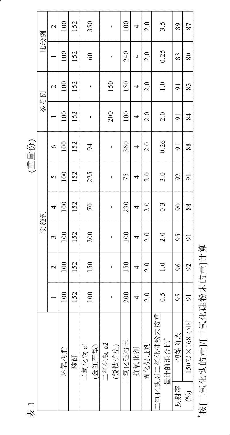
[0062] Examples 1 to 6, Reference Examples 1 and 2, Comparative Examples 1 and 2
[0063] The ingredients shown in Table 1 below were mixed in the ratios shown therein, then melt mixed in a beaker, aged, then cooled to room temperature and ground to prepare the desired finely powdered epoxy resin composition.
[0064] The thus-produced epoxy resin compositions of Examples and Comparative Examples were analyzed to measure their reflectance (initial stage, after standing at high temperature for a long period of time). The results are shown in Table 1 below.
[0065] Reflectivity
[0066] Under predetermined curing conditions (conditions: forming at 150° C. for 4 minutes + curing at 150° C. for 3 hours), the epoxy resin composition was formed into a test piece with a thickness of 1 mm; and at the initial stage and at 150° C. The total reflectance of the test piece (cured material) was measured after standing still for 168 hours. As a tester, a spectrophotometer V-670 manufact...
PUM
| Property | Measurement | Unit |
|---|---|---|
| softening point | aaaaa | aaaaa |
| particle size | aaaaa | aaaaa |
| particle size | aaaaa | aaaaa |
Abstract
Description
Claims
Application Information