Thin-film transistor, array substrate and manufacturing method and display device thereof

A technology for thin film transistors and array substrates, which is applied in the field of display device manufacturing, and can solve problems such as affecting the performance of oxide semiconductor thin films, incomplete coverage, and damage.

Active Publication Date: 2012-08-29
BOE TECH GRP CO LTD
View PDF5 Cites 55 Cited by
  • Summary
  • Abstract
  • Description
  • Claims
  • Application Information

AI Technical Summary

Problems solved by technology

[0025] It can be seen from the above manufacturing method that the most widely used manufacturing method of the existing OTFT array substrate is the above-mentioned 6-time patterning process to form the gate metal layer, semiconductor layer, etch barrier layer, data line metal layer, passivation layer, etc. However, complex processes such as film formation, exposure, and etching after the semiconductor active layer will directly affect the p

Method used


Image

  • Thin-film transistor, array substrate and manufacturing method and display device thereof
  • Thin-film transistor, array substrate and manufacturing method and display device thereof
  • Thin-film transistor, array substrate and manufacturing method and display device thereof

Examples


Embodiment Construction

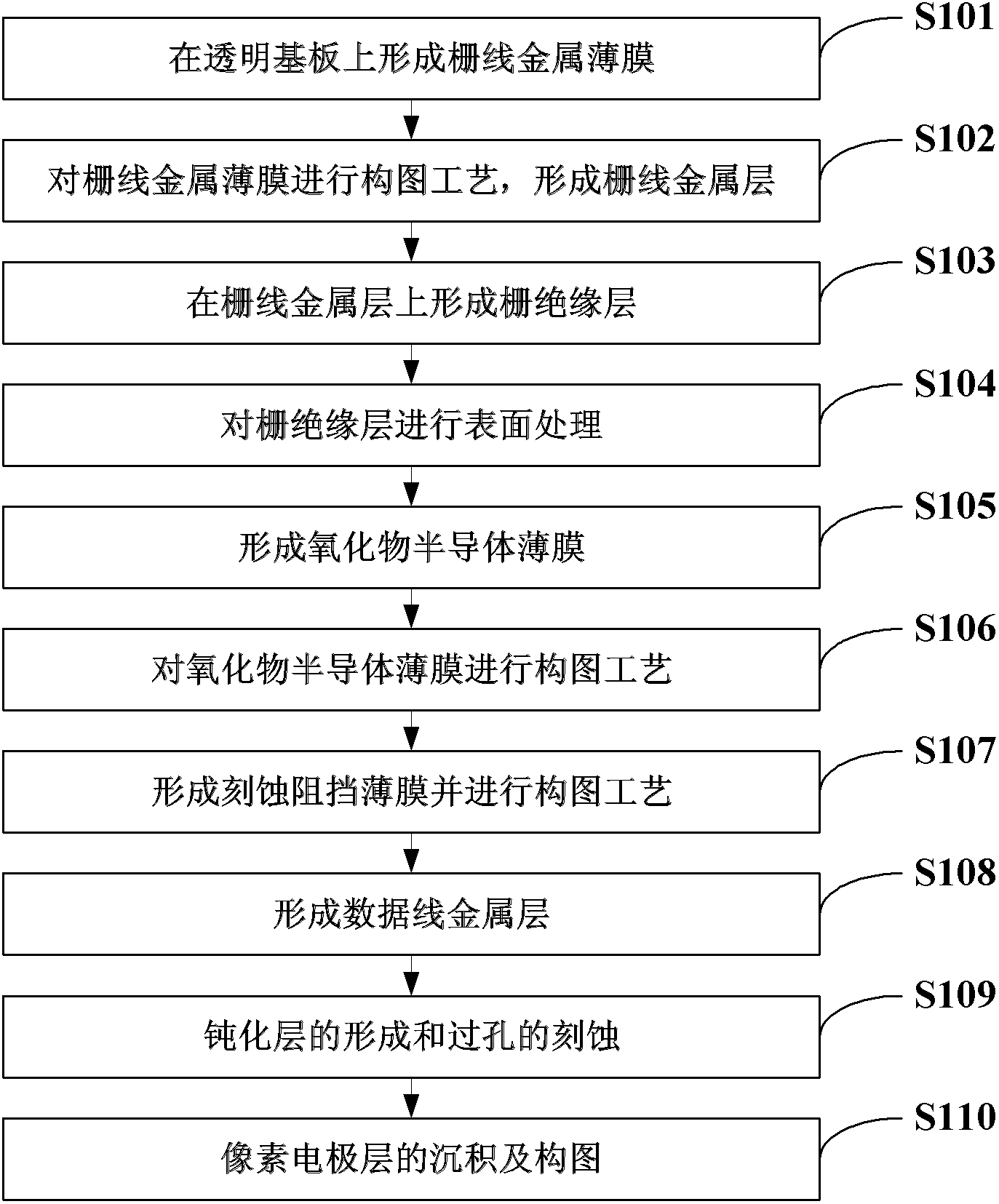
[0063] The following will clearly and completely describe the technical solutions in the embodiments of the present invention with reference to the accompanying drawings in the embodiments of the present invention. Obviously, the described embodiments are only some, not all, embodiments of the present invention. Based on the embodiments of the present invention, all other embodiments obtained by persons of ordinary skill in the art without making creative efforts belong to the protection scope of the present invention.

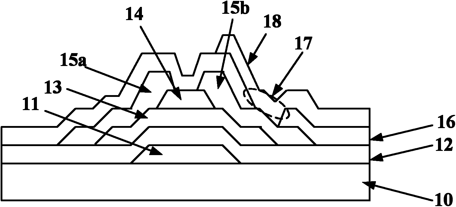
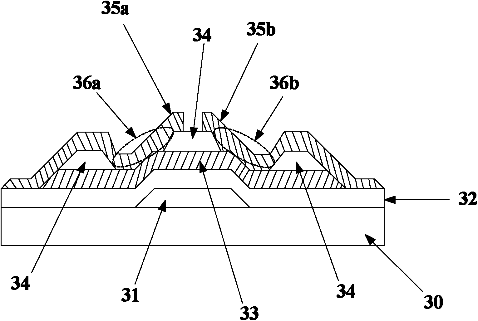
[0064] An embodiment of the present invention provides a thin film transistor, such as Figure 3A Or as shown in 3B, it includes a transparent substrate 30, a gate 31, a gate insulating layer 32, a semiconductor active layer 33, an etching stopper layer 34, a source electrode 35a and a drain electrode 35b, wherein, by patterning the etching stopper layer process, the etch barrier layer 34 covers the semiconductor active layer 33, and a first via hole 36a and a...


PUM


Abstract

The embodiment of the invention provides a thin-film transistor, an array substrate and a manufacturing method and a display device thereof, relating to the technical field of displays, and aiming to avoid damage of an active layer of a semiconductor caused by direct illumination and etching, thereby improving the performance of a thin-film transistor (TFT) device. The thin-film transistor comprises a grid electrode, a grid insulation layer, a semiconductor active layer, an etching blocking layer, a source electrode and a drain electrode; the etching blocking layer covers the semiconductor active layer; and a first through hole and a second through hole are formed on the etching blocking layer; the source electrode of the thin film transistor is in contact with the semiconductor active layer through the first through hole; and the drain electrode of the thin film transistor is in contact with the semiconductor active layer through the second through hole. According to the embodiment of the invention, the manufacturing method is used for manufacturing the thin-film transistor and the array substrate, as well as the display device which utilizes the thin-film transistor and the array substrate.

Description

technical field [0001] The invention relates to a display device manufacturing technology, in particular to a thin film transistor, an array substrate, a manufacturing method thereof, and a display device. Background technique [0002] The initial research on OTFT (Oxide Thin Film Transistor) technology is a technology developed to reduce the energy consumption of active display devices, making display devices thinner, lighter, and faster in response. Around the beginning of the 21st century began to move towards the trial stage. With the characteristics of ultra-thin, light weight, low energy consumption, and its own light-emitting characteristics, a new generation of organic light-emitting liquid crystal panels OLED (Organic Light-Emitting Diode, Organic Light-Emitting Diode) that can provide more vivid colors and clearer images is officially launched. Go to the practical stage. Oxide thin film transistor technology is also regarded as the most promising technology that ...

Claims


Application Information

Patent Timeline
IPC IPC(8): H01L29/786H01L27/12H01L21/77
CPCH01L29/7869H01L27/1225H01L29/66969H01L27/1248H01L27/1259H01L27/124H01L29/41733H01L29/78606
Inventor 袁广才
Owner BOE TECH GRP CO LTD
Why Eureka
Try Eureka