

Pixel circuit and drive method thereof as well as display panel
A pixel circuit and drive transistor technology, applied in static indicators, instruments, etc., can solve problems such as poor display effect, current difference, different OLED operating voltage, etc., to achieve good display effect and improve uniformity
- Summary
- Abstract
- Description
- Claims
- Application Information
AI Technical Summary
Problems solved by technology
Method used
Image

Examples
Embodiment 1
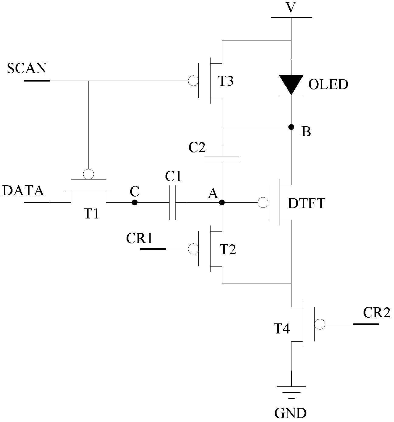
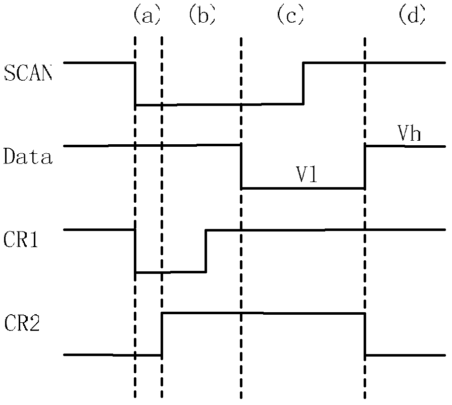
[0032] In this embodiment, the 5T2C circuit is used to compensate Vth, so that I=K(Vgs-Vth) of the drive tube 2 Regardless of the threshold voltage Vth of the drive transistor, the current flowing through the OLED is consistent and the uniformity is improved. Specific as figure 2 As shown, the pixel circuit of this embodiment includes: gate line SCAN, data line DATA, power line V, first signal line CR1, second signal line CR2, ground electrode GND, first switching transistor T1, second switching transistor T2 , a third switching transistor T3, a fourth switching transistor T4, a driving transistor DTFT, a first storage capacitor C1, a second storage capacitor C2 and an OLED device. Among them, five transistors are all P-type transistors.
[0033] The gate of the first switching transistor T1 is connected to the gate line SCAN, the source is connected to the data line DATA, and the drain is connected to the first end of the first storage capacitor C1. The storage capacitor ...
Embodiment 2
[0044] This embodiment provides a display panel, including the pixel circuit in Embodiment 1, the pixel circuit is formed on an array substrate, and the array substrate is provided with a plurality of data lines and gate lines, and a plurality of data lines and gate lines A plurality of the above-mentioned pixel circuits are defined; the array substrate further includes a driver chip for providing timing signals for gate lines, data lines, first signal lines and second signal lines, and power supply signals for power lines.
PUM
 Abstract
Description
Claims
Application Information