Composite anodic bonding method

A composite anode and anodic bonding technology, used in precision positioning equipment, microstructure technology, microstructure devices, etc., can solve the problems that restrict the wide application of interface activation composite anode bonding process, strict wet chemical activation process conditions, and bonding efficiency. Low-temperature and other problems, to achieve the effect of low-temperature high-efficiency anodic bonding, good controllability of bonding performance, and convenient operation

Inactive Publication Date: 2012-09-12
SUZHOU UNIV
View PDF4 Cites 14 Cited by
  • Summary
  • Abstract
  • Description
  • Claims
  • Application Information

AI Technical Summary

Problems solved by technology

However, the high temperature makes anodic bonding prone to the following problems: First, the bonding efficiency is low. During the bonding process of silicon / glass, the high temperature will cause the gas in the glass micropores to expand, decompose, and overflow, forming gas at the bonding interface. Floor
However, the current plasma activation environment conditions are strict and require special expensive plasma equipment. The process conditions of wet chemical activation are strict and the process is complicated, resulting in the problems of complex process and poor controllability of these activation methods, which restrict the interface activation composite anodic bonding. Wide application of technology

Method used


Image

  • Composite anodic bonding method
  • Composite anodic bonding method
  • Composite anodic bonding method

Examples


Embodiment Construction

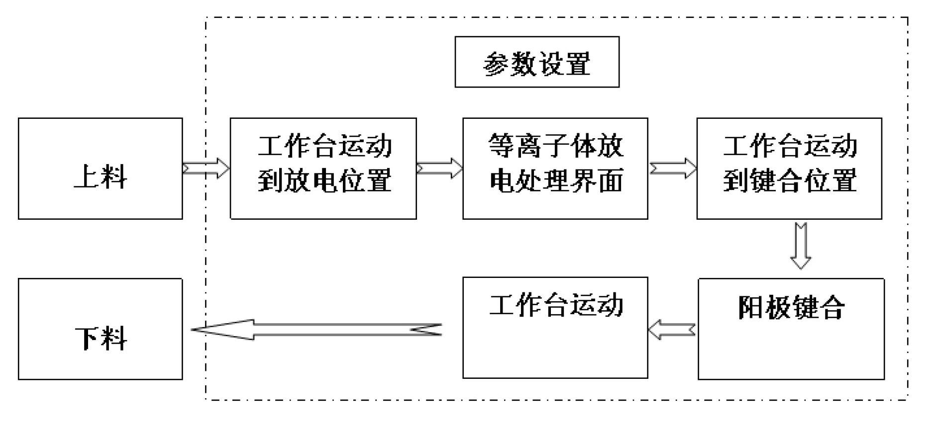
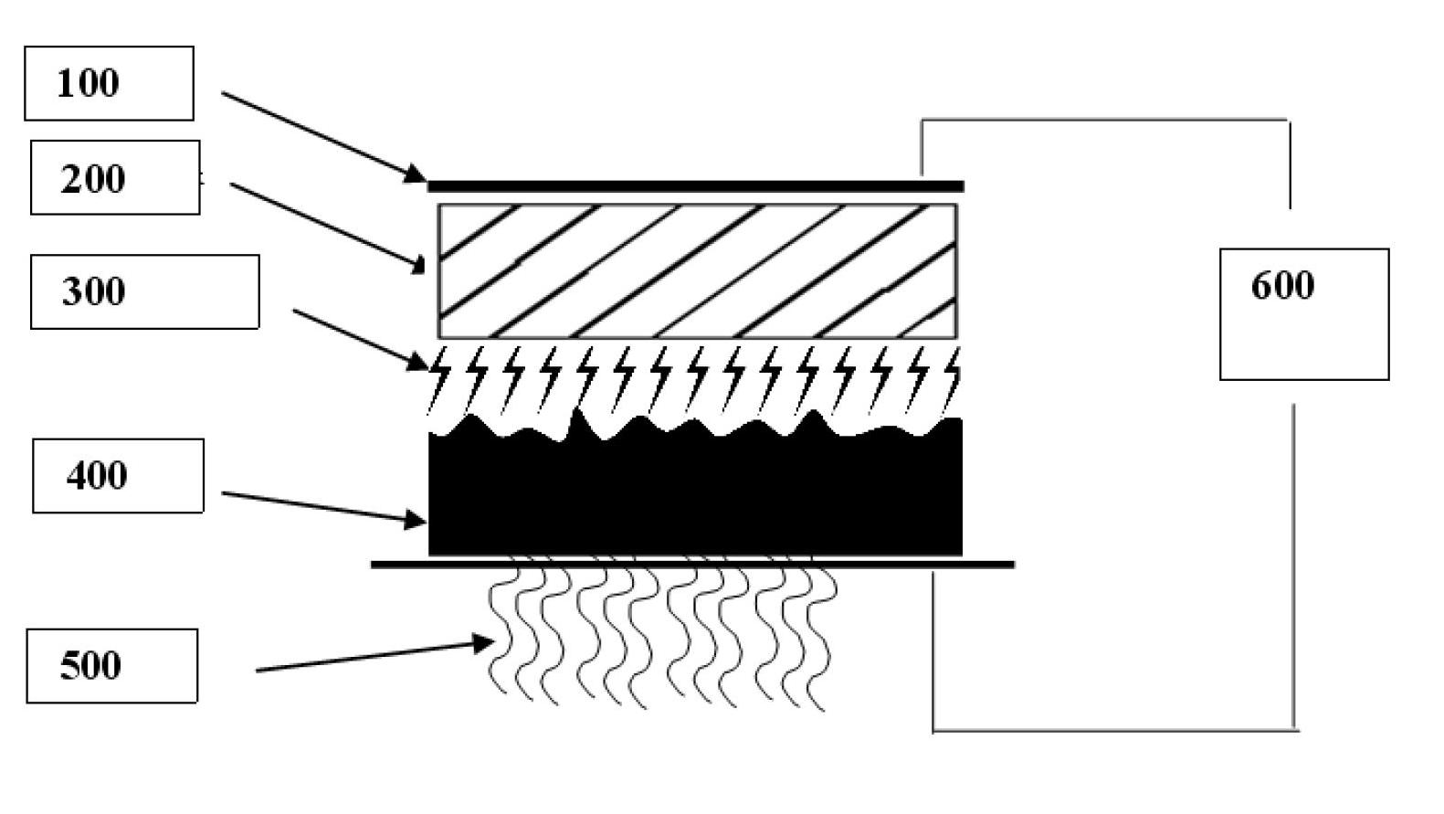
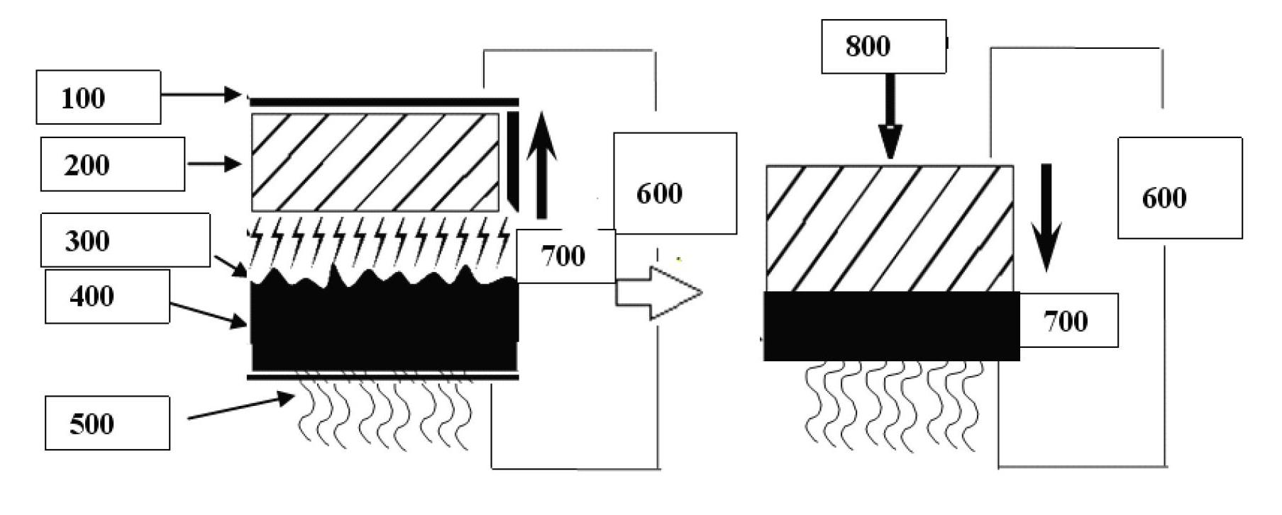
[0034] In the prior art, conventional anodic bonding has low bonding efficiency. In the silicon / glass bonding process, high temperature will cause the gas in the glass pores to expand, decompose, and overflow, forming a gas layer at the bonding interface, and poor gas drainage will form pore defects at the interface. In order to make the gas smooth At present, point electrodes and multi-point electrodes are widely used in wafer-level bonding. When this type of electrode is used, the distribution of the external electric field on the bonding interface is not uniform, and the bonding can only be gradually advanced from the electrode position to the edge. It takes a long time to complete the bonding of the whole piece, and the bonding efficiency is low.

[0035] At present, the step-by-step pretreatment anodic bonding equipment used in the prior art is complicated, and the process is difficult to realize; moreover, the two processes of pretreatment and bonding are not in the same s...


PUM


Abstract

The invention relates to a composite anodic bonding method. According to the composite anodic bonding method, two working procedures of bonding interface pretreatment through dielectric-barrier plasma discharge and anodic bonding are finished on the same station. The composite anodic bonding method comprises the following steps of: clamping a silicon wafer or glass on a fixed workbench, and clamping a vitreous body or the silicon wafer on a movable workbench; simultaneously heating the two workbenches to 250-350 DEG C, wherein the movable workbench drives the vitreous body or the silicon wafer to move so as to urge a 1-500mum gap to be formed between bonded faces; generating plasma discharge in the gap under the action of DC 500-2000V or AC500-2000V / 10-1000Hz discharge voltage, and carrying out activating treatment for 0.1-20s on bonding interfaces through plasma discharge; then removing discharge voltage, simultaneously the movable workbench drives the vitreous body or the silicon wafer to move so that the bonding interfaces are mutually in touch and form 0.1-50g pressure, and finally finishing the anodic bonding under the action of DC500-2000V bonding voltage. According to the composite anodic bonding method, as the two working procedures of bonding interface activation pretreatment through dielectric-barrier plasma discharge and anodic bonding are integrated and finished on the same station, the bonding controllability is good, and the operation is convenient.

Description

Technical field [0001] The invention belongs to the technical field of microelectromechanical systems and integrated circuit packaging, and in particular relates to a composite anode bonding method. Background technique [0002] Anode bonding technology plays an important role in the production, assembly, and packaging of MEMS (Micro-Electro-Mechanical Systems) devices. It is the core technology for connecting multiple silicon processing technologies and is to achieve cross-over in three-dimensional space. One of the basic methods of complex MEMS structures such as structure and multilayer structure. [0003] At present, the anodic bonding is realized by the method of high temperature (400~500℃) and high voltage (1000~2000V). The basic principle is to connect the silicon wafer and glass to the two poles of the high-voltage power supply, and under certain temperature, voltage and pressure The physical and chemical reaction at the bonding interface promotes the opening and closing o...

Claims


Application Information

Patent Timeline
Patent Type & Authority Applications(China)
IPC IPC(8): B81C3/00
Inventor 潘明强陈涛刘吉柱陈立国孙立宁
Owner SUZHOU UNIV
Why Eureka
Try Eureka