Programmable visual chip-based visual image processing system

A visual image and processing system technology, applied in the field of visual image processing systems based on programmable visual chips, can solve the problems of large chip area, lack of advanced image processing functions, and inability to achieve fast and flexible wide-area processing.

Active Publication Date: 2012-09-12
INST OF SEMICONDUCTORS - CHINESE ACAD OF SCI
View PDF3 Cites 89 Cited by
  • Summary
  • Abstract
  • Description
  • Claims
  • Application Information

AI Technical Summary

Problems solved by technology

[0006] (1) Each pixel unit includes a photosensitive element, a readout circuit and a processing circuit. The chip area is large, which greatly limits the resolution and filling rate, and the original image quality is poor; and because the photosensitive element and the readout circuit are analog circuits , so the processing circuit often uses analog circuits, resulting in poor reliability and flexibility of image processing
[0007] (2) These pixel units are arranged in a two-dimensional array and work in the single instruction multiple data (SIMD) mode, which can realize full-pixel parallel image acquisition and local processing, but cannot realize fast and flexible wide-area processing;
[0008] (3) The above-mentioned programmable vision chip architecture working in SIMD mode supports low-level image processing and some intermediate-level image processing, but lacks advanced image processing functions, especially the simple and intuitive fast feature recognition ability similar to human brain nerves, so it must A complete visual image system can only be formed with the help of an external general-purpose processor, which limits the application of visual chips in some embedded occasions that have strict requirements on volume, power consumption and cost

Method used


Image

  • Programmable visual chip-based visual image processing system
  • Programmable visual chip-based visual image processing system
  • Programmable visual chip-based visual image processing system

Examples


Embodiment Construction

[0083] In order to make the object, technical solution and advantages of the present invention clearer, the present invention will be described in further detail below in conjunction with specific embodiments and with reference to the accompanying drawings.

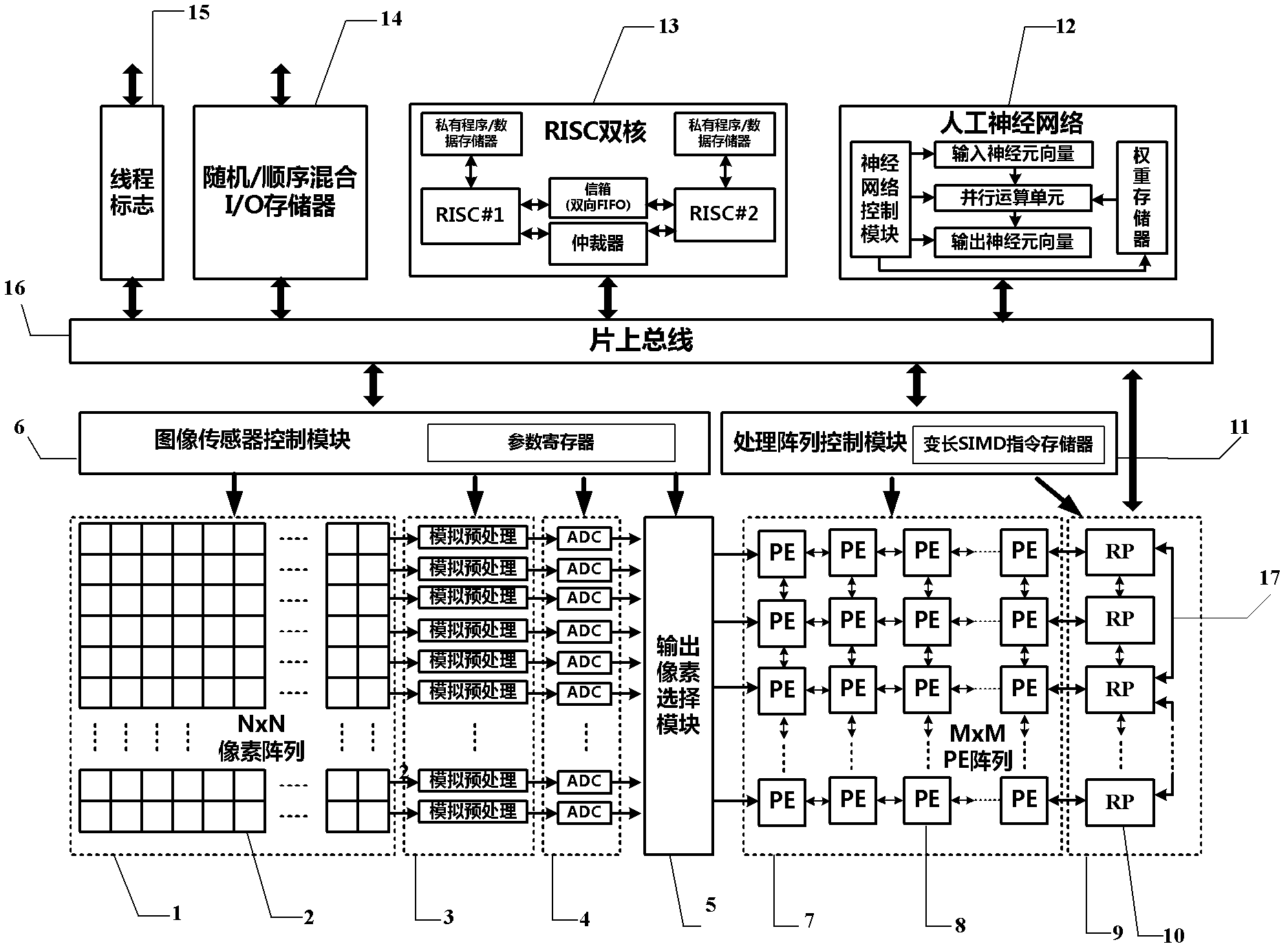
[0084] Such as figure 1 as shown, figure 1 It is a schematic structural diagram of a visual image processing system based on a programmable visual chip provided by the present invention, and the system includes two parts: an image sensing module and a multi-stage parallel digital image processing module. Wherein the image sensor module includes an N×N pixel array, an N×1 parallel analog preprocessing array, an N×1 parallel analog-to-digital conversion unit (ADC) array, an output pixel selection module and an image sensor control module, in this embodiment , N=256, which can reach the standard resolution in applications such as machine vision. Multi-level parallel digital image processing module includes M×M pixel-level ...


PUM


Abstract

Disclosed in the invention is a programmable visual chip-based visual image processing system, comprising an image sensor and a multilevel parallel digital processing circuit. The image sensor mainly includes a pixel array, an analog preprocessing circuit array and an analog-to-digital conversion circuit array; and the digital processing circuit consists of a parallel processing unit array with an M*M pixel level, a parallel processing unit array with M*1 rows, an on-chip artificial neural network and a reduced instruction processor dual-core subsystem. According to the provided system, high quality image collection with high speed and multilevel parallel image processing are realized and several high-speed intelligent visual application can be realized by programming; and compared with a traditional image system, the provided system has advantages of high speed, high integration, low power consumption and low cost. Moreover, the invention brings forward an embodiment for realizing the above-mentioned system as well as several high-speed intelligent visual image processing algorithms based on the embodiment. High-speed motion detection, high-speed gesture identification and rapid face detection are included; and the processing speed can reach 1000 frames per second. Therefore, a requirement of high-speed real-time processing can be met.

Description

technical field [0001] The present invention relates to the technical field of programmable visual chips and image processing, in particular to a visual image processing system based on programmable visual chips, which has the advantages of high speed, high integration, low power consumption, and low cost, and can be applied to various embedded High-speed real-time visual image processing system realizes various intelligent visual image applications including high-speed target tracking, natural human-computer interaction, environmental monitoring, intelligent transportation, robot vision, etc. Background technique [0002] The traditional visual image processing system includes a discrete camera and a general-purpose processor (or digital signal processor (DSP)), the camera uses an image sensor to acquire images, and serially transmits a large amount of raw image data acquired to the general-purpose processor or DSP processing, there are severe bandwidth constraints due to s...

Claims


Application Information

Patent Timeline
Patent Type & Authority Applications(China)
IPC IPC(8): H04N5/335H04N5/357H04N5/378
Inventor 石匆吴南健龙希田杨杰秦琦
Owner INST OF SEMICONDUCTORS - CHINESE ACAD OF SCI
Why Eureka
Try Eureka