Device and method for automatic optical detection

A technology of automatic optical detection and actual position, which is used in measuring devices, material analysis by optical means, scientific instruments, etc. The effect of storage, improving processing power, and real-time output

Active Publication Date: 2012-09-19
上海赫立智能机器有限公司
View PDF5 Cites 25 Cited by
  • Summary
  • Abstract
  • Description
  • Claims
  • Application Information

AI Technical Summary

Problems solved by technology

In the PCBA (Printed Circuit Board Assembly, printed circuit board assembly) production process, since the components on the PCB have been showing a trend of continuous miniaturization and densification, it is impossible to rely on the traditional manual visual inspection method to check the layout on the PCB. Precision components perform fast, reliable and stable appearance defect detection, and accurate detection records cannot be kept. Among them, common defects include: missing parts, offsets, wrong parts, reverse poles, short circuits, lack of tin, and excess tin , False soldering, standing on the side, erecting a monument, reverse sticking, damage, multiple pieces, tin beads, gold finger scratches, dents, printed circuit board scratches, poor incoming materials, etc.
[0008] First, because only the area with components on the inspected PCB is photographed, it is impossible to detect the appearance defects in the area without components on the inspected PCB, such as multiple p

Method used


Image

  • Device and method for automatic optical detection
  • Device and method for automatic optical detection
  • Device and method for automatic optical detection

Examples


Embodiment Construction

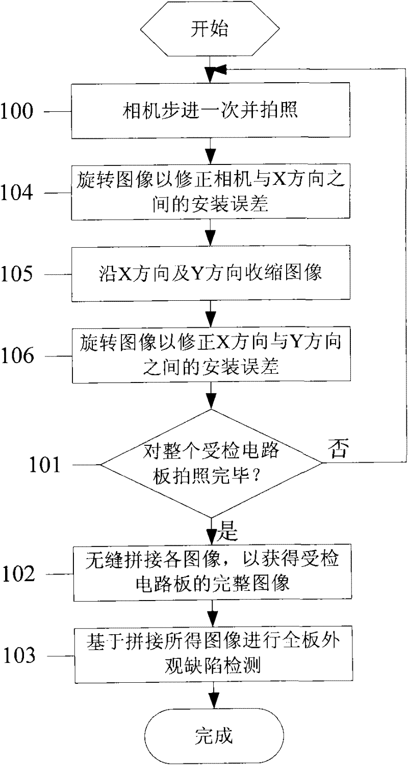
[0031] Hereinafter, preferred embodiments of the present invention are given in conjunction with the drawings to illustrate the technical solutions of the present invention in detail.

[0032] The automatic optical inspection device of the present invention is used for detecting the appearance defects of a circuit board under inspection, such as a PCB. The AOI device includes an image acquisition unit and an image processing unit. The component structure of the image acquisition unit can be the same as the existing image acquisition unit, and the hardware structure of the image processing unit can also be the same as the existing image processing unit. The processing unit is the same.

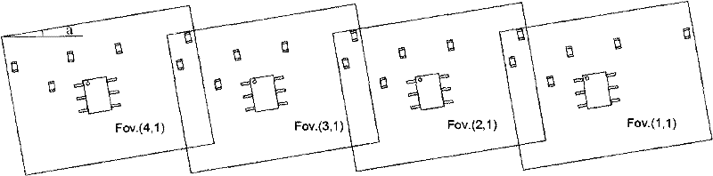
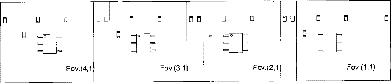
[0033] However, in the present invention, the image acquisition unit is no longer to take selective partial and partial photographs of the inspected circuit board, but to take a comprehensive partial photograph of the entire surface of the inspected circuit board. Specifically, the image acquisitio...


PUM


Abstract

The invention discloses a device and a method for automatic optical detection, wherein the device comprises an image acquiring unit and an image processing unit; the image acquiring unit is used for performing stepping two-dimensional scanning movement relative to a detected circuit board, and photographing the detected circuit board once after stepping every time, wherein the sum of images acquired by the photographing every time covers the complete surface of the detected circuit board; and the image processing unit is used for seamlessly splicing the images acquired by the photographing every time into a complete image of the detected circuit board, and performing image difference analysis between the complete image acquired by the splicing and the design standards of the detected circuit board, so as to detect the apparent defects of the detected circuit board. Via the device and the method disclosed by the invention, the complete image of the detected circuit board can be acquired, so that an omni-directional accurate detection can be performed on the detected circuit board.

Description

Technical field [0001] The invention relates to an automatic optical inspection device (AOI, Automated Optical Inspector), in particular to an automatic optical inspection device and an automatic optical inspection method realized by the automatic optical inspection device. Background technique [0002] PCB (Printed Circuit Board, printed circuit board) has a wide range of applications, and can be seen everywhere in the interior of electronic products such as mobile phones, telephones, televisions, computers, automobiles, copiers, printers, and air conditioners. In the PCBA (Printed Circuit Board Assembly, printed circuit board assembly) production process, because the components on the PCB have been showing a trend of continuous miniaturization and density, it is no longer possible to rely on traditional manual visual inspection methods to lay out the PCB Precise components perform fast, reliable and stable appearance defect inspection, and can not save accurate inspection recor...

Claims


Application Information

Patent Timeline
IPC IPC(8): G01N21/956
Inventor 程克林
Owner 上海赫立智能机器有限公司
Why Eureka
Try Eureka