Unlock instant, AI-driven research and patent intelligence for your innovation.

Semiconductor memory system

A memory system and semiconductor technology, applied in the direction of semiconductor devices, static memory, read-only memory, etc., to achieve the effect of suppressing bending

Inactive Publication Date: 2012-09-19
KK TOSHIBA
View PDF4 Cites 4 Cited by
  • Summary
  • Abstract
  • Description
  • Claims
  • Application Information

AI Technical Summary

Problems solved by technology

Non-volatile semiconductor storage elements are arranged along the long side direction on the surface layer side of the substrate

Method used


Image

  • Semiconductor memory system
  • Semiconductor memory system
  • Semiconductor memory system

Examples


Embodiment Construction

[0027] Hereinafter, the semiconductor memory system according to the embodiment will be described in detail with reference to the drawings. In addition, this invention is not limited to these embodiment.

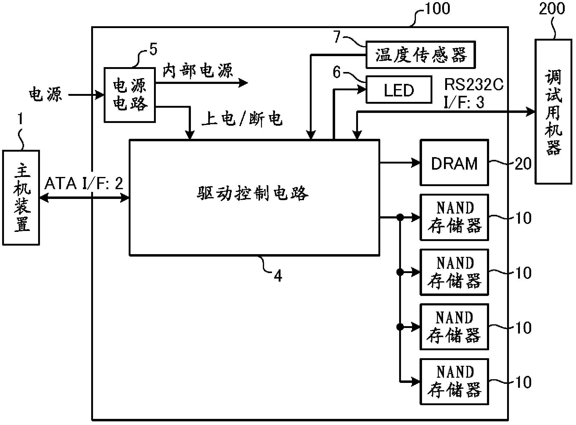
[0028] figure 1 It is a block diagram showing a configuration example of the semiconductor memory system according to the first embodiment. The semiconductor memory system 100 is connected to a host device (hereinafter, simply referred to as a host) 1 such as a personal computer or a CPU core via a memory connection interface such as a SATA interface (ATA I / F) 2 , and is used as an external memory of the host 1 . As the host 1, a CPU of a personal computer, a CPU of an imaging device such as a still camera or a video camera, and the like can be cited. Furthermore, the semiconductor memory system 100 can transmit and receive data between the debugging devices 200 via a communication interface 3 such as an RS232C interface (RS232C I / F).

[0029] The semiconductor memory sys...


PUM


Abstract

According to one embodiment, a semiconductor memory system includes a substrate, a plurality of elements and an adhesive portion. The substrate has a multilayer structure in which wiring patterns are formed, and has a substantially rectangle shape in a planar view. The elements are provided and arranged along the long-side direction of a surface layer side of the substrate. The adhesive portion is filled in a gap between the elements and in a gap between the elements and the substrate, where surfaces of the elements are exposed.

Description

[0001] Associate application [0002] This application enjoys the benefit of priority of Japanese Application Patent No. 2011-058140 filed on March 16, 2011, the entire contents of which are incorporated herein by reference. technical field [0003] Generally, the present embodiments relate to semiconductor memory systems. Background technique [0004] Conventionally, a semiconductor memory system in which a nonvolatile semiconductor memory element such as a NAND flash memory is mounted on a substrate on which a connector is formed has been used. Furthermore, in addition to the nonvolatile semiconductor memory element, the semiconductor memory system includes a volatile semiconductor memory element and a controller for controlling the nonvolatile semiconductor memory element and the volatile semiconductor memory element. [0005] In such a semiconductor memory system, the shape and size of the substrate may be restricted depending on the usage environment, specifications, e...

Claims


Application Information

Patent Timeline
IPC IPC(8): G11C16/06H01L27/10
CPCH05K1/18H01L23/49822H01L23/3121G11C16/06H05K1/0298H05K1/0271H05K1/0225H01L23/34H05K2201/09681H01L23/00H05K2201/09136H01L27/10H05K3/305H05K2201/10159H01L2924/0002H01L2924/00Y02P70/50H10B69/00G11C5/02H01L23/3142H01L23/49838H01L23/552H01L23/562H01L25/0655H05K1/181H01L23/5286H01L25/18H01L25/50
Inventor 增渕勇人木村直树松本学森本丰太
Owner KK TOSHIBA
Features
  • R&D
  • Intellectual Property
  • Life Sciences
  • Materials
  • Tech Scout
  • Unparalleled Data Quality
  • Higher Quality Content
  • 60% Fewer Hallucinations
Learn More