Double-drain type CMOS magnetic field induction transistor and fabricating method thereof

A magnetic field sensing and transistor technology, which is applied in the field of CMOS magnetic field sensor transistors, can solve the problems of complex Hall plate structure, high power consumption, and unfavorable realization of large-scale magnetic field sensing array systems.

Inactive Publication Date: 2012-09-19
HUNAN SEEKSUNS OPTOELECTRONICS TECH
View PDF3 Cites 5 Cited by
  • Summary
  • Abstract
  • Description
  • Claims
  • Application Information

AI Technical Summary

Problems solved by technology

However, in order to obtain greater sensitivity to magnetic field sensing, the CMOS Hall plate needs to provide a greater bias current, so the power consumption is relatively large
In addition, the structure of the Hall disk is relatively complex, which is not conducive to the realization of a large-scale magnetic field induction array system

Method used


Image

  • Double-drain type CMOS magnetic field induction transistor and fabricating method thereof
  • Double-drain type CMOS magnetic field induction transistor and fabricating method thereof
  • Double-drain type CMOS magnetic field induction transistor and fabricating method thereof

Examples


Embodiment Construction

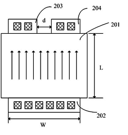
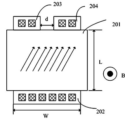
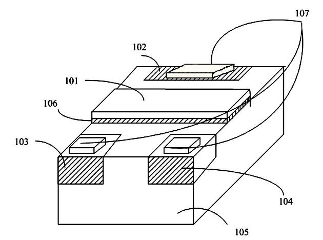
[0018] Such as figure 1 , 2 As shown, the CMOS double-drain magnetic field induction transistor of the present invention includes a P-type substrate 105, two n+ drain doped regions 103, 104, an n+ source doped region 102, a polysilicon gate 101, and silicon dioxide oxide layer 106, metal contact hole 107. First, a silicon dioxide oxide layer and a polysilicon gate are formed on a P-type substrate, and then a source n+ heavily doped region and a drain n+ heavily doped region are respectively formed on both sides of the polysilicon gate, wherein the drain n+ is heavily doped Divide into two identical areas separated by a certain distance.

[0019] The specific manufacturing process of the CMOS double-drain magnetic field induction transistor is described as follows:

[0020] (1) growing a silicon dioxide layer 106 on the P-type substrate 105;

[0021] (2) Removing the silicon dioxide on the diffusion windows of the source n+ doped region 102 and the drain n+ doped regions 10...


PUM


Abstract

The invention discloses a double-drain type CMOS (Complementary Metal-Oxide-Semiconductor) magnetic field induction transistor and a fabricating method thereof. The double-drain type CMOS magnetic field induction transistor comprises a P type substrate, two n+ drain doped region, an n+ source doped region, a p+ substrate contact doped region, a polycrystalline silicon gate and a silicon dioxide oxide layer. The method comprises the following steps of: firstly, growing the silicon dioxide oxide layer and the polycrystalline silicon gate on the P type substrate; and secondly, generating a source n+ heavily doped region and a drain n+ heavily doped region and the p+ substrate contact doped region on the two sides of the polycrystalline silicon gate, wherein the drain n+ heavily doped region is divided into two same regions having a certain distance therebetween. The double-drain structure is capable of realizing induction to a magnetic field under the action of the magnetic field to current carriers in an inversion layer formed under the transistor and is completely compatible with standard CMOS process; and simultaneously, compared with a magnetic sensor of a hall disc structure, the double-drain type CMOS magnetic field induction transistor is lower in power consumption.

Description

technical field [0001] The invention relates to a CMOS magnetic field sensor transistor, in particular to a CMOS magnetic field sensor transistor with a double-drain type magnetic field induction transistor structure and a manufacturing method thereof. Background technique [0002] The Hall effect has been widely used in the design of magnetic field sensors, especially for integration with standard CMOS processes. A common practice at present is to use the CMOS Hall plate structure, that is, to let the bias current pass through a square semiconductor material (such as an N-well resistor). When a magnetic field is applied vertically to the semiconductor surface, a voltage difference will be generated on both sides of the semiconductor, thereby The induction to the magnetic field is realized. However, in order to obtain greater sensitivity to magnetic field sensing, the CMOS Hall plate needs to provide a greater bias current, so the power consumption is relatively large. In ...

Claims


Application Information

Patent Timeline
Patent Type & Authority Applications(China)
IPC IPC(8): H01L27/22H01L21/82
Inventor 郭晓雷金湘亮
Owner HUNAN SEEKSUNS OPTOELECTRONICS TECH
Why Eureka
Try Eureka