Monocrystalline silicon nano-film flexible transient electronic device, preparation method and application

A transient electronic device, nano-film technology, applied in electrical components, nanotechnology, nanotechnology and other directions, can solve problems such as inability to adapt to the application environment

Active Publication Date: 2018-11-16
FUDAN UNIV
View PDF9 Cites 5 Cited by
  • Summary
  • Abstract
  • Description
  • Claims
  • Application Information

AI Technical Summary

Problems solved by technology

However, due to the limitations of organic trigger materials, current transient electronic devices are mostly unable to adapt to high temperature (>150°C) application environments such as vehicles, aerospace, and energy mining.

Method used


Image

  • Monocrystalline silicon nano-film flexible transient electronic device, preparation method and application
  • Monocrystalline silicon nano-film flexible transient electronic device, preparation method and application
  • Monocrystalline silicon nano-film flexible transient electronic device, preparation method and application

Examples


Embodiment 1

[0064] Embodiment 1 Sensitive information / technical anti-disclosure protection device

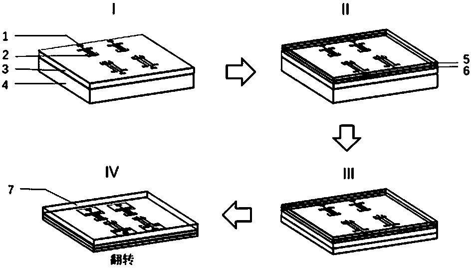
[0065] Field-effect transistors are the basis of logic and storage circuits, and almost any integrated circuit system can be prepared in the form of a flexible transient device by using the preparation process and the transient electronic technology involved in the present invention. Taking the most basic logic device unit field effect transistor in integrated circuits as an example, its physical photos and device structure are as follows: figure 2 , 3 shown. The device includes a metal electrode 1, a silicon nanofilm 2, a thermally oxidized silicon dioxide layer 3, a flexible substrate layer 5, a bottom-up spin-coated polyimide layer (~5 μm), a polydimethylsiloxane layer (~5 μm), polyimide film (12.5 μm), poly-α-methylstyrene 6, its thickness is about 4 μm; electrode pass 7 on thermally oxidized silicon dioxide layer; gate oxide layer 8 of the device, SiO from top to bottom 2 (72 nm),...

Embodiment 2

[0069] Example 2 Single-crystal silicon nano-thin film transient photodetector with ultra-high switching ratio

[0070] Using the standard process parameters introduced in the preparation method of the invention, the preparation and thinning of silicon nanometer thin film phototransistors on the SOI wafer are completed, and flexible devices are obtained.

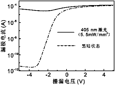
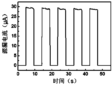
[0071] pass Figure 9 The output characteristic curves for the device shown are operating and Figure 10 The photoelectric response characteristics under gate voltage regulation shown in , can confirm the bias working state required for the device to achieve ultra-high switching ratio. Under a certain gate voltage, the output current of the transistor increases significantly with the drain voltage first, and then tends to be stable. It can be seen from the figure that as the irradiation intensity increases, the photocurrent of the transistor increases almost linearly. It can be seen that changing the gate voltage can sign...

Embodiment 3

[0075] Example 3 On-Chip Integrated Self-Destructive High-Temperature Circuit Protection Device

[0076] Using the idea of ​​device first and then thinning introduced in the present invention, silicon nanometer thin film integrated circuits are prepared on SOI wafers according to standard technology, and a PAMS transient failure trigger layer is added under silicon nanometer thin film transistors in a specific area.

[0077] Compared with bulk silicon materials, the source and drain regions of silicon nano-thin film transistors are completely depleted, and only the side is in contact with the channel, which eliminates the p-n junction in the vertical direction and significantly reduces the leakage of the transistor under high-temperature operating conditions; at the same time, the device adopts resistance High-temperature polyimide film flexible substrate, and add spin-coated polyimide stress buffer film layer in multi-layer structure. The above structural features can meet th...


PUM

PropertyMeasurementUnit
thicknessaaaaaaaaaa
thicknessaaaaaaaaaa
thicknessaaaaaaaaaa

Abstract

The invention belongs to the technical field of micro-nano electronic devices, and specifically relates to a monocrystalline silicon nano-film flexible transient electronic device, a preparation method and an application. The invention adopts a preparation method of firstly preparing a device and then performing transfer, that is, a monocrystalline silicon nano-film electronic device / array prepared according to the standard semiconductor process is integrally transferred to a polyimide film flexible substrate with a transient functional layer. The preparation method has the advantages of compatibility with the current IC process, arbitrary adjustment of the structure scale and suitability for industrial large-scale production. According to the invention, the channel energy band is regulated and controlled through a gate, and the ratio of light current and dark current of the device can exceed 10<6>. The self-destructive transient process of a heating trigger device is realized throughadding the PAMS functional layer in the preparation process. The invention lays a foundation for obtaining high-sensitivity flexible photoelectric detectors and transient devices capable of adapting to a high temperature environment in a large scale in the fields such as on-chip integrated circuit protection, information security and sensing / control systems.

Description

technical field [0001] The invention relates to a single-crystal silicon nano-film flexible transient electronic device, a preparation method and an application, and belongs to the technical field of micro-nano electronic devices. Background technique [0002] With the continuous development of microelectronics technology, the size characteristics and integration of devices are constantly approaching the theoretical limit. Due to the unique physical and chemical properties and flexible characteristics brought by the ultra-thin thickness, the two-dimensional nano-film has great application potential in many fields such as wearable, implantable, and environmental protection. Among them, high-performance field-effect transistors and photodetectors, as the basis of logic units and detection and sensing parts of these flexible devices, have become key research directions in this field. [0003] Although organic semiconductor materials are naturally flexible, their electrical pro...

Claims


Application Information

Patent Timeline
Patent Type & Authority Applications(China)
IPC IPC(8): H01L31/11H01L31/112H01L31/18B82Y15/00
CPCB82Y15/00H01L31/1105H01L31/1129H01L31/1804Y02P70/50
Inventor 梅永丰李恭谨宋恩名黄高山
Owner FUDAN UNIV
Why Eureka
Try Eureka