Patterned substrate of LED chip and LED chip

A technology for LED chips and patterned substrates, applied in electrical components, circuits, semiconductor devices, etc., can solve problems such as failure to prepare new patterns, GaN growth quality damage, etc., to improve internal quantum efficiency and epitaxy quality , The effect of excellent light extraction efficiency

Inactive Publication Date: 2012-09-26
SOUTH CHINA UNIV OF TECH
View PDF6 Cites 3 Cited by
  • Summary
  • Abstract
  • Description
  • Claims
  • Application Information

AI Technical Summary

Problems solved by technology

[0005] Even though patterned substrates have greatly improved the light extraction efficiency of LEDs, in terms of pattern design, since the emergence of hemispherical patterns, researchers have not been able to prepare new patterns with more light-emitting advantages; and on the optimization of pattern size, Solving the trade-off between size reduction and damage to GaN growth quality, ensuring better epitaxy quality under the premise of improving light extraction efficiency, and improving LED performance in a real sense still need to be studied

Method used


Image

  • Patterned substrate of LED chip and LED chip
  • Patterned substrate of LED chip and LED chip
  • Patterned substrate of LED chip and LED chip

Examples


Embodiment 1

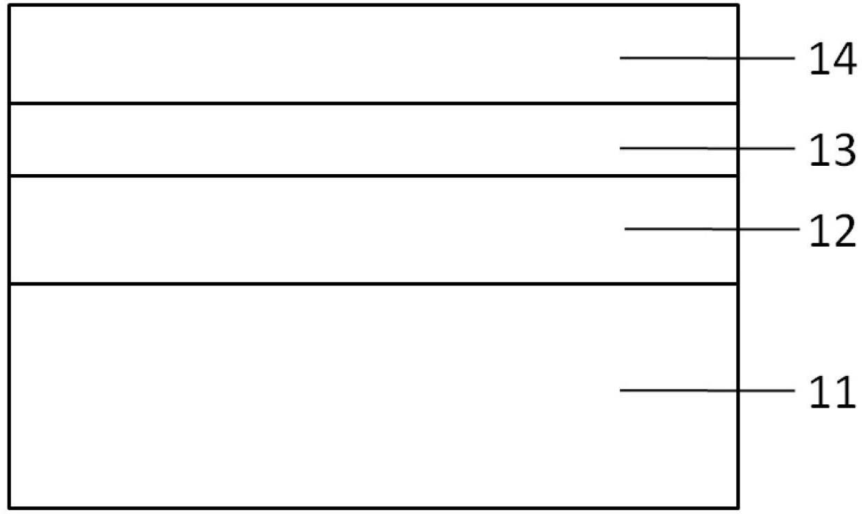
[0026] figure 1 Be the schematic diagram of the LED chip of this embodiment, as figure 1 As shown, it consists of a patterned sapphire substrate 11, an N-type GaN layer 12, an MQW quantum well layer 13, and a P-type GaN layer 14 arranged in sequence.

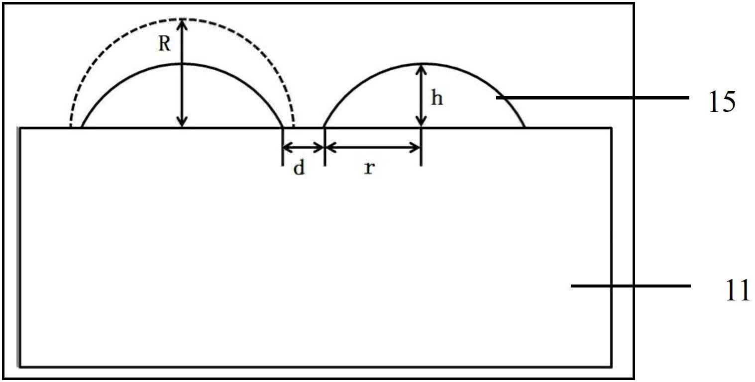
[0027] Such as figure 2 As shown, in the patterned substrate of the LED chip of this embodiment, the pattern of the substrate is composed of a plurality of spherical caps of the same shape arranged on the surface of the substrate, and the height h of each spherical cap is the radius of the sphere corresponding to the spherical cap. 75% of R; the edge spacing d of adjacent spherical caps is 30% of the bottom surface radius r of the spherical caps; the radius R of the sphere corresponding to the spherical caps in this embodiment is 2 μm; the plurality of spherical caps of the same shape use as image 3 The rectangular arrangement shown.

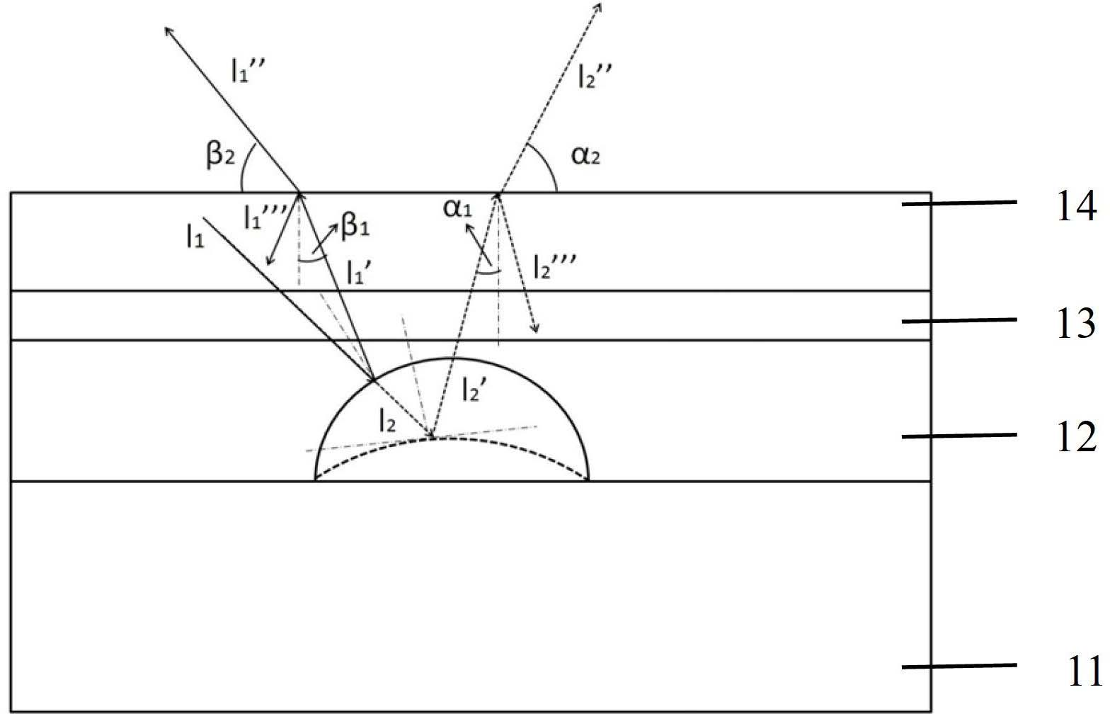
[0028] Figure 4 It is a schematic diagram of changing the optical path of the spherica...

Embodiment 2

[0030] In the patterned substrate of the LED chip of this embodiment, the pattern of the substrate is composed of a plurality of spherical caps of the same shape arranged on the surface of the substrate, and the height h of each spherical cap is 85% of the radius R of the sphere corresponding to the spherical cap. %; the edge spacing d of adjacent spherical caps is 50% of the bottom surface radius r of the spherical caps; the radius R of the sphere corresponding to the spherical caps in this embodiment is 3.5 μm; the plurality of spherical caps with the same shape are used as Figure 5 The hexagonal arrangement shown.

Embodiment 3

[0032] In the patterned substrate of the LED chip of this embodiment, the pattern of the substrate is composed of a plurality of spherical caps of the same shape arranged on the surface of the substrate, and the height h of each spherical cap is 80% of the radius R of the sphere corresponding to the spherical cap. %; the edge spacing d of adjacent spherical caps is 40% of the radius r of the bottom surface of the spherical caps; the radius R of the sphere corresponding to the spherical caps in this embodiment is 3 μm; the plurality of spherical caps with the same shape adopts a hexagonal arrangement Way.


PUM


Abstract

The invention discloses a patterned substrate of an LED chip and an LED chip. Patterns of the substrate consist of a plurality of identically-shaped spherical caps arranged on the surface of the substrate, the height h of each spherical cap is 75-85 percent of the radius R of the sphere corresponding to the spherical cap, and the distance d between the edges of the adjacent spherical caps is 30-50 percent of the radius r of the bottom surface of the spherical caps. Compared with the prior art, the patterned substrate has better light extraction efficiency than a substrate with hemispherical patterns with the same bottom surface radius, is simpler in actual processing and facilitates popularized application.

Description

technical field [0001] The invention relates to an LED chip, in particular to a patterned substrate of the LED chip and the LED chip. Background technique [0002] Patterned substrate technology is a recent research hotspot in the field of GaN-based LEDs on sapphire substrates. Since its pattern evolution, it has significantly improved the LED light extraction effect and epitaxy quality, and has become an important way to improve LED performance. [0003] The improvement of the optical performance of the LED by the substrate pattern is reflected in two aspects: on the one hand, the pattern changes the trajectory of the light through scattering / reflection, so that the incident angle of the light exiting at the interface becomes smaller (less than the critical angle of total reflection), and then it is transmitted out. Improve the light extraction rate; on the other hand, the pattern can also make the subsequent GaN growth appear the effect of lateral epitaxy, reduce crystal ...

Claims


Application Information

Patent Timeline
Patent Type & Authority Applications(China)
IPC IPC(8): H01L33/00
Inventor 李国强王海燕周仕忠林志霆
Owner SOUTH CHINA UNIV OF TECH
Why Eureka
Try Eureka