Ion implantation method and manufacturing method of semiconductor device

An ion implantation, semiconductor technology, used in semiconductor/solid state device manufacturing, electrical components, circuits, etc.

Inactive Publication Date: 2012-10-10
SEMICON MFG INT (BEIJING) CORP
View PDF5 Cites 0 Cited by
  • Summary
  • Abstract
  • Description
  • Claims
  • Application Information

AI Technical Summary

Problems solved by technology

[0010] The present invention provides an ion implantation method and a manufacturing method of a semiconductor device to improve ion scattering in the photoresist layer in the existing ion implantation process. process impact

Method used


Image

  • Ion implantation method and manufacturing method of semiconductor device
  • Ion implantation method and manufacturing method of semiconductor device
  • Ion implantation method and manufacturing method of semiconductor device

Examples


Embodiment Construction

[0029] The specific embodiments of the present invention will be described in detail below in conjunction with the accompanying drawings.

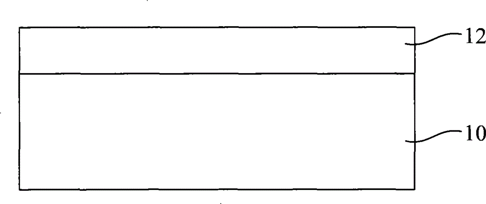
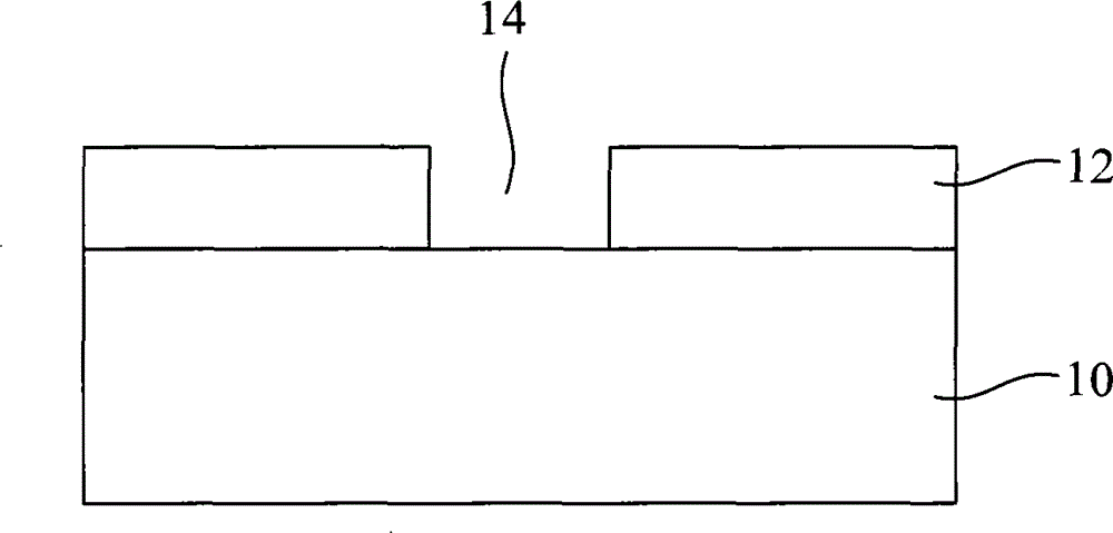
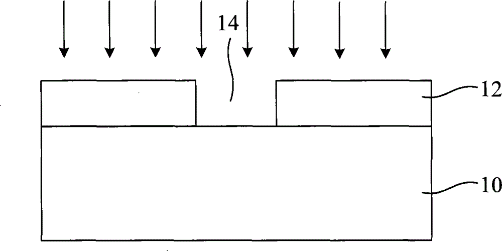
[0030] In the manufacturing method of metal oxide semiconductor devices, a multi-step ion implantation process is required, such as the formation of well regions (N well or P well), the formation of source and drain electrodes, the formation of lightly doped regions, etc., all need to be realized through ion implantation processes. The ion implantation process plays an important role in the manufacturing process of metal oxide semiconductor devices.

[0031] The process conditions of the ion implantation process have a great influence on the electrical properties of the formed metal oxide semiconductor device. How to control, adjust and change the ion implantation process conditions so that the implanted ions after the ion implantation process can reach the target dose, and are located at The target region, so that the electrical character...


PUM


Abstract

An ion implantation method comprising the following steps: providing a semiconductor substrate; forming a photoresist layer on the semiconductor substrate; patterning the photoresist layer to form an opening which is provided with inclined sidewall and used for defining an ion implantation region in the semiconductor substrate; implanting ion on the semiconductor substrate at the bottom of the opening; wherein, the included angel between the sidewall and the surface of the region to be implanted is an obtuse angle. The invention also provides a manufacturing method of semiconductor device andcan reduce or eliminate ions implanted in the semiconductor substrate caused by scatting of the photoresist layer of the ion during the ion implantation.

Description

technical field [0001] The invention relates to the technical field of semiconductor manufacturing, in particular to an ion implantation method and a manufacturing method of a semiconductor device. Background technique [0002] Metal oxide semiconductor devices are widely used in fields such as computers, communications, and storage due to their low power consumption and fast response characteristics. A typical metal oxide semiconductor device includes a gate, source and drain. In order to improve the electrical performance of the metal oxide semiconductor device, some metal oxide semiconductor transistors also have a drain extension region (Drain extend region). [0003] The source, drain and the above-mentioned drain extension region are generally formed by ion implantation process, therefore, the process conditions of ion implantation determine the electrical characteristics of the formed source, drain and drain extension region, and then determine the formed metal oxide...

Claims


Application Information

Patent Timeline
Patent Type & Authority Patents(China)
IPC IPC(8): H01L21/266H01L21/336
Inventor 丁宇居建华
Owner SEMICON MFG INT (BEIJING) CORP
Why Eureka
Try Eureka